Organic electroluminescence display apparatus

a technology of electroluminescence display and organic el, which is applied in the direction of instruments, discharge tubes luminescnet screens, static indicating devices, etc., can solve the problems of reducing the life-expectation of the organic el display apparatus, affecting the performance of the organic el element, and causing large parallax

Inactive Publication Date: 2007-02-08
HITACHI DISPLAYS
View PDF4 Cites 46 Cited by
  • Summary
  • Abstract
  • Description
  • Claims
  • Application Information

AI Technical Summary

Benefits of technology

[0038] The respective units and methods according to the present invention allow the implementation of the long life-expectancy and high-definition performance of the

Problems solved by technology

However, when the light is extracted via the insulating substrate, thickness of the insulating substrate causes a large parallax to occur.
If, however, it is wished that such a structure is to be implemented, a high-heat process at the time of forming the active elements in the second layer or thereafter causes damage to occur in the first-layer organic EL elements.
This damage lowers life-expectancy of the organic EL display apparatus.
This nec

Method used


Image

  • Organic electroluminescence display apparatus
  • Organic electroluminescence display apparatus
  • Organic electroluminescence display apparatus

Examples


embodiment 1

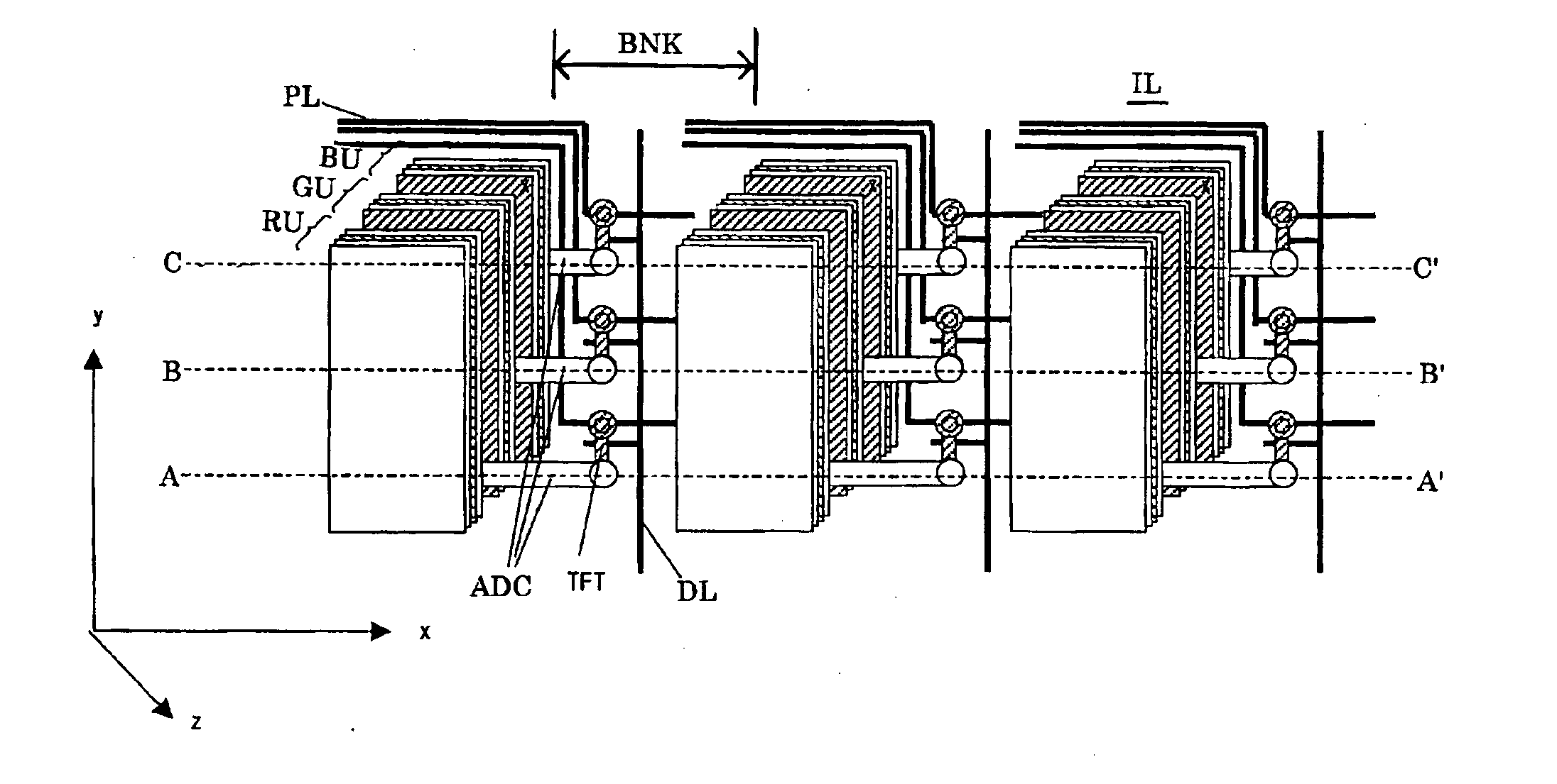
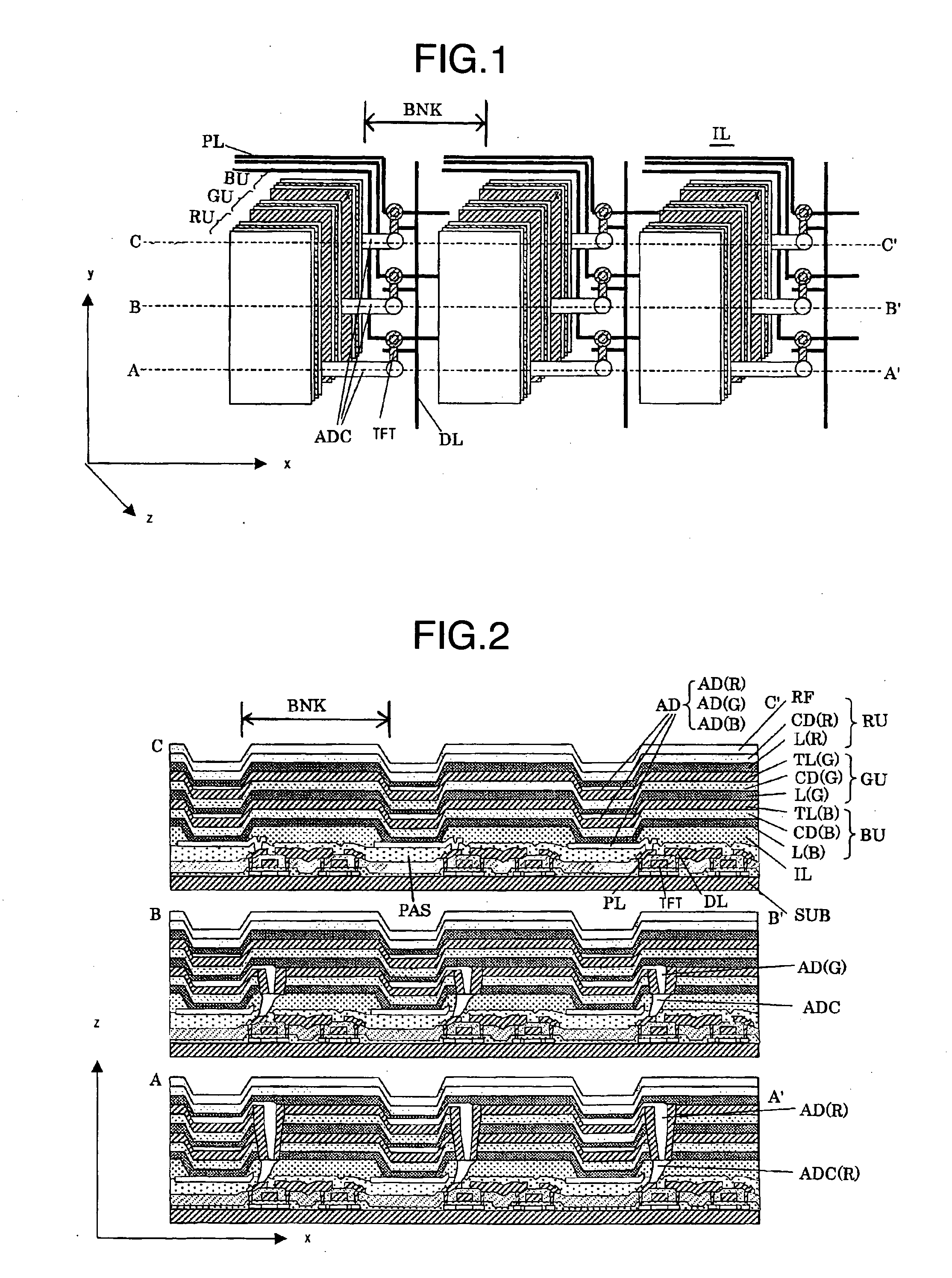
[0059]FIG. 1 is a conceptual diagram for explaining a first embodiment of the present invention. Also, FIG. 2 illustrates cross-sectional views acquired by cutting off the first embodiment along an A-A′ line, a B-B′ line, and a C-C′ line in FIG. 1. The first embodiment is the so-called bottom-emission pixel display apparatus for emitting out display light from an insulating-substrate SUB side. Each of the primary colors, i.e., red (R), green (G), and blue (B), corresponds to a unit pixel (i.e., a subpixel). These three color unit pixels form one color main pixel. In FIG. 1, the insulating substrate (hereinafter, glass substrate) SUB illustrated in FIG. 2 exists in the back of the paper surface. An active pixel circuit where thin-film transistors are used as the active elements is fabricated into the main surface (i.e., inner surface) of this glass substrate SUB. An inter-layer insulating film IL is formed in the upper layer of this active pixel circuit.

[0060] On the inter-layer ins...

embodiment 2

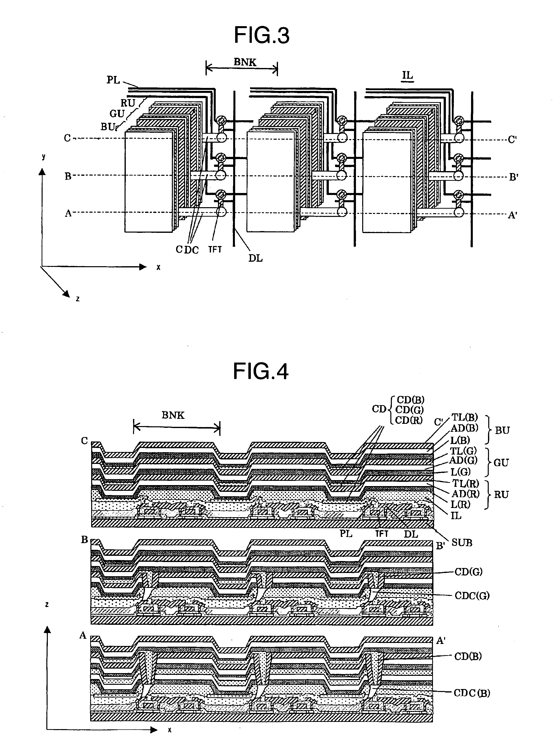
[0073]FIG. 3 is a conceptual diagram for explaining a second embodiment of the present invention. Also, FIG. 4 illustrates cross-sectional views acquired by cutting off the second embodiment along an A-A′ line, a B-B′ line, and a C-C′ line in FIG. 3. The second embodiment is the so-called top-emission pixel display apparatus for emitting out display light from the opposite side to the insulating substrate SUB. In this organic EL display apparatus, the red (R) organic EL element RU, the green (G) organic EL element GU, and the blue (B) organic EL element BU are multi-layered in this order from the glass-substrate SUB side. Similarly to the first embodiment, the three unit pixels are located within the area of one unit pixel. This location makes it possible to accomplish implementation of the higher-definition performance as compared with the conventional location where the respective organic EL elements are located in the substrate-surface direction.

[0074] In FIG. 4, the red (R) org...

embodiment 3

[0079]FIG. 5 is a conceptual diagram for explaining a third embodiment of the present invention. Also, FIG. 6 illustrates cross-sectional views acquired by cutting off the third embodiment along an A-A′ line, a B-B′ line, and a C-C′ line in FIG. 5. The third embodiment is basically the same as the second embodiment except a point that the organic light-emitting layers L (R), L (G), and L (B) in the second embodiment are formed by evaporation using a mask. Namely, the organic light-emitting layers L (R), L (G), and L (B) configuring the red, green, and blue organic EL elements RU, GU, and BU with the three-layer structure are evaporated using the mask in only the aperture portion of the pixel (i.e., between the banks BNKs). The other configurations are the same as those in the second embodiment.

[0080] In the configuration of the third embodiment, basically the same materials are used as those in the second embodiment. Moreover, the configuration is embodied in basically the same fil...


PUM


Abstract

There is provided a high-definition and small-parallax active-driving organic EL display apparatus capable of avoiding complication of manufacturing processes and skyrocketing in component and material expenses. A plurality of organic EL elements BU, GU, and RU are multi-layered in a single subpixel area. All of active elements (i.e., thin-film transistors TFTs) to be connected to the multi-layered organic EL elements are formed between an insulating substrate SUB and the layer of the organic EL element BU which is the most proximate to this insulating substrate. This configuration makes it possible to avoid the second-layer or upper organic EL elements GU and RU from being damaged by the high-heat processing in the manufacturing processes. Accordingly, it becomes possible to implement long life-expectancy of the organic EL display apparatus. Also, inter-layer spacing between the organic EL elements can be made narrower. Consequently, it becomes possible to make the parallax exceedingly smaller.

Description

INCORPORATION BY REFERENCE [0001] The present application claims priority from Japanese application JP2005-189703 filed on Jun. 29, 2005, the content of which is hereby incorporated by reference into this application. BACKGROUND OF THE INVENTION [0002] 1. Field of the Invention [0003] The present invention relates to an organic EL display apparatus. More preferably, it relates to an active-matrix organic EL display apparatus where a plurality of organic EL elements are multi-layered on an insulating substrate. [0004] 2. Description of the Related Art [0005] As flat-panel display apparatuses, such display apparatuses as liquid-crystal display apparatuses (LCD), plasma display apparatuses (PDP), field emission display apparatuses (FED), and organic EL display apparatuses (OLED) have been already at the practical-commercialization stage, or are now at the practical-commercialization research stage. Of these display apparatuses, the organic EL display apparatuses in particular are excee...

Claims


Application Information

Patent Timeline
IPC IPC(8): G09G3/10
CPCG09G3/3233G09G3/3258G09G2300/0452G09G2300/0842H01L51/5278G09G2320/029G09G2320/043H01L27/3244G09G2320/0242H10K59/32H10K59/123
Inventor ITO, NAOYUKIYAMANAKA, KANAE
Owner HITACHI DISPLAYS
Why Eureka
Try Eureka