Liquid crystal display panel, thin film transistor array substrate and detection methods therefor

a thin film transistor array and display panel technology, applied in non-linear optics, instruments, optics, etc., can solve the problems of large power consumption, limited crt, and further minimize the occupied space of crt, and achieve the effect of simplifying the detection circui

Inactive Publication Date: 2007-02-08
CHUNGHWA PICTURE TUBES LTD
View PDF3 Cites 53 Cited by
  • Summary
  • Abstract
  • Description
  • Claims
  • Application Information

AI Technical Summary

Benefits of technology

[0010] Accordingly, the present invention is directed to a thin film transistor array substrate with a simpler layout.

Problems solved by technology

However, the larger power consumption and the higher radiation features of the CRT contradict to the green environment concept.
In addition, to further minimize the occupied space of a CRT is limited.
As a result, the CRT can not meet the market trend of a lightweight, thin, short, compact, appealing and low-power consumption product.
If the pixel unit is abnormal, it needs to repair the abnormal device (such as thin film transistor or pixel electrode .
It should be noted that the detection circuit is complex, and the layout region of the panel would narrow down because of the detection circuit.
Furthermore, the external factors such as manual transportation or changes in the environment may lead to the static charges accumulation in the liquid crystal display panel.
When the static charges exceed a definite amount, an electrostatic discharge may occur and this would damage the lines or the thin film transistor on the thin film transistor array substrate.
So, it will make the layout of the peripheral circuit region more complex and the space for the layout may not be enough.
And this doesn't help simplify the fabrication process and promote the productivity efficiency.

Method used


Image

  • Liquid crystal display panel, thin film transistor array substrate and detection methods therefor
  • Liquid crystal display panel, thin film transistor array substrate and detection methods therefor
  • Liquid crystal display panel, thin film transistor array substrate and detection methods therefor

Examples


first embodiment

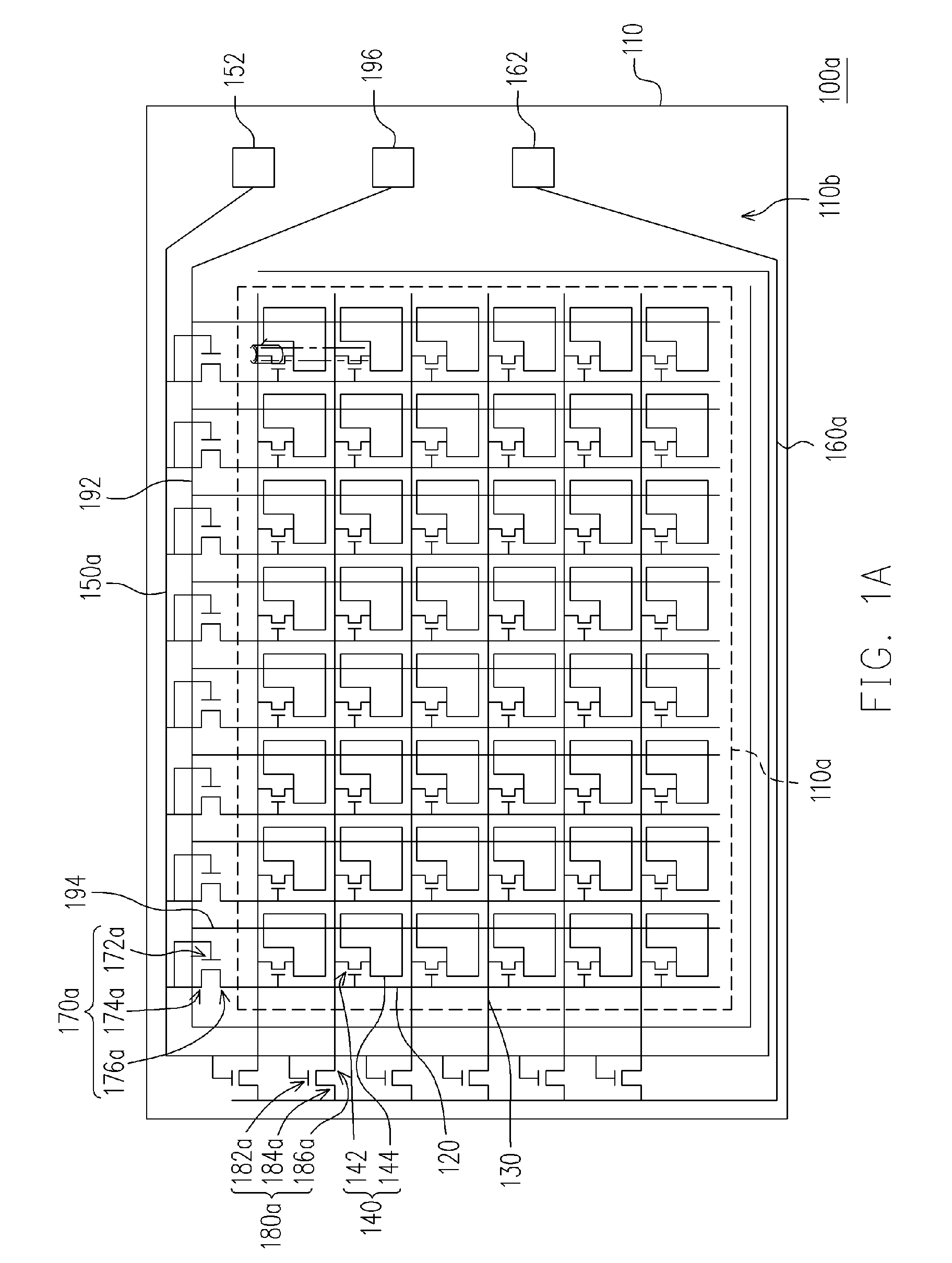
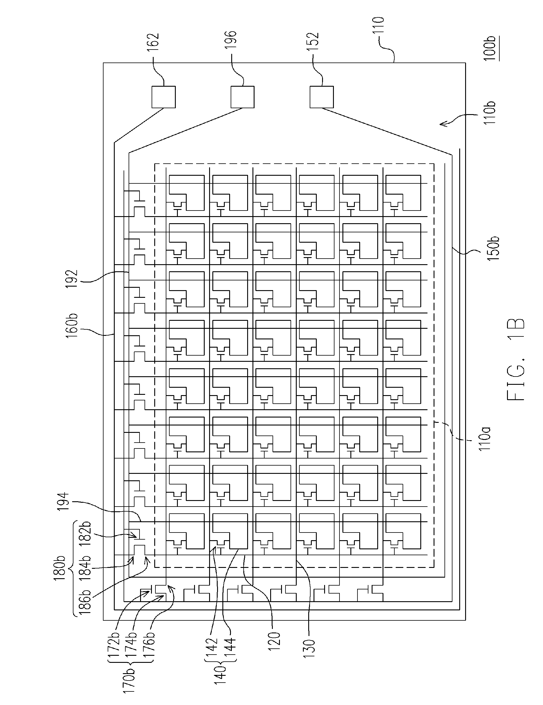
[0056]FIGS. 1A and 1B are schematic views showing a thin film transistor array substrate according to the first embodiment of the present invention. First, please refer to FIG. 1A, the thin film transistor array substrate 100a comprises a substrate 110, a plurality of scan lines 120, a plurality of data lines 130, a plurality of pixel units 140, an inner anti-static ring 150a, a circuit 160a, a plurality of first thin film transistors 170a and a plurality of second thin film transistors 180a. The substrate 110 comprises a display region 110a and a peripheral circuit region 110b. The substrate 110 may comprise a quartz substrate, a glass substrate or other transparent substrate.

[0057] The scan lines 120 and data lines 130 are arranged on the substrate 110, and the pixel units 140 are arranged on the display region 110a. Besides, each pixel unit 140 is controlled by the corresponding scan line 120 and data line 130. Further, each pixel unit 140 comprises an active device 142 and a pi...

second embodiment

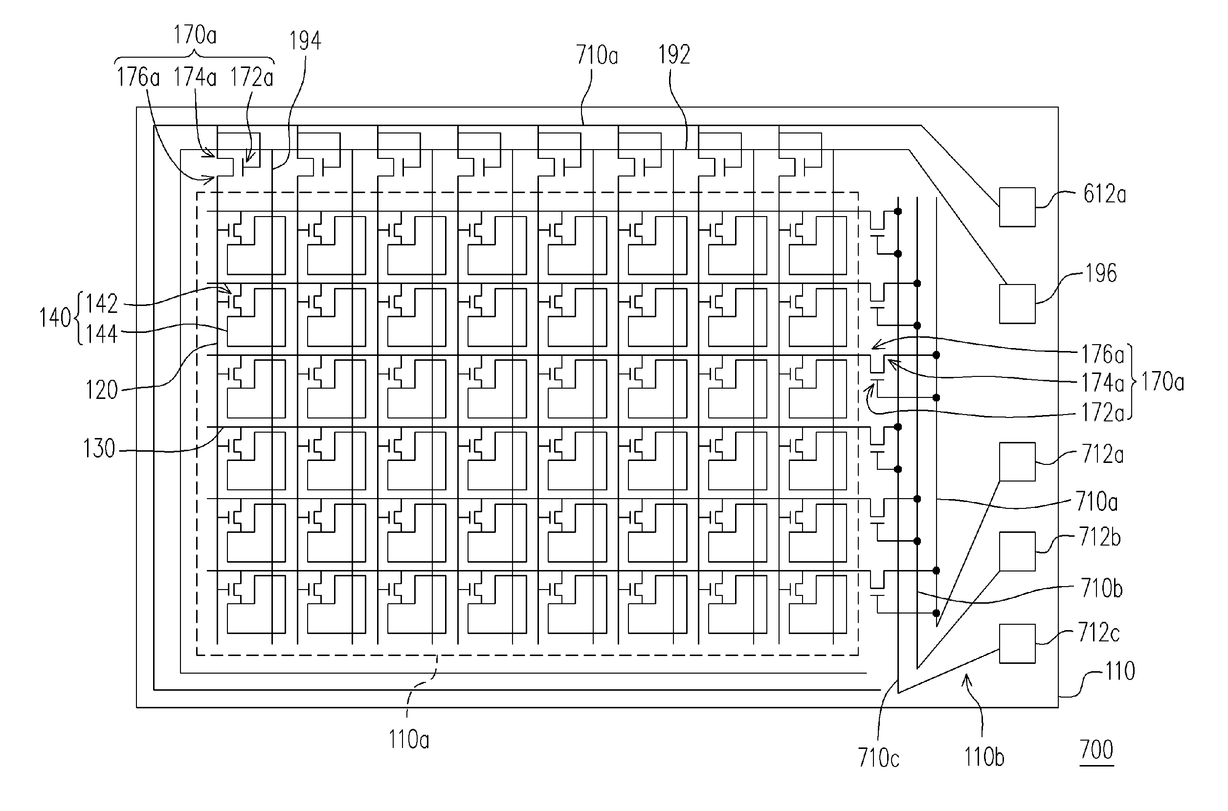
[0069]FIG. 3 is a schematic view showing a thin film transistor array substrate according to the second embodiment of the present invention. Please refer to FIG. 3, the content of FIG. 3 is similar to that of FIG. 1, the difference is that the circuit 510 of the thin film transistor array substrate 500 comprises lines 510a, 510b and 510c. Besides, the detection pad 512a, 512b and 512c can be arranged at one end of the lines 510a, 510b and 510c in order to input signals or measure signals.

[0070] For a short circuit detection, the detection method for the thin film transistor array substrate 500 comprises the step of transmitting current signals to the scan lines 120 through the detection pad 152, the inner anti-static ring 150a and the first transistors 170a. Then, each detection pad 512a, 512b and 512c is measured respectively in order to determine that a short circuit occurs between the scan lines 120 and data lines 130 connected to the detection pad 512a, 512b and 512c. For examp...

third embodiment

[0073]FIG. 4 is a schematic view showing a thin film transistor array substrate according to the third embodiment of the present invention. Please refer to FIG. 4, the content of FIG. 4 is similar to that of FIG. 1, the difference is that a portion of the first transistors 170a of the thin film transistor array substrate 600 are connected to the inner anti-static ring 610a and the scan line 120 respectively and the other portion of the first transistors 170a are connected to the inner anti-static ring 610b and the data line 130. In other words, the thin film transistor array substrate 600 doesn't comprise a circuit similar to the circuit 160a shown in FIG. 1A. Besides, the detection pads 612a and 612b can also be arranged at one end of the inner anti-static rings 610a and 610b.

[0074] Similarly, the above mentioned detection method can also apply to determine that if a short circuit occurs between the common line 194 and the scan line 120. In brief, a current signal is transmitted t...


PUM

PropertyMeasurementUnit
currentaaaaaaaaaa
poweraaaaaaaaaa
electrical testaaaaaaaaaa

Abstract

A thin film transistor (TFT) array substrate including a substrate, pixel units, scan and data lines, inner anti-static rings, first and second thin film transistors is provided. The pixel units are arranged on a display region of the substrate, and the scan and data lines are arranged on the substrate. Each pixel unit is controlled by the corresponding scan and data line. The inner anti-static rings, the first and second TFTs are arranged on a peripheral circuit region of the substrate around the display region. The gate and source of each first TFT are connected to one part of the inner anti-static ring, and the drain of each first TFT is connected to the scan line respectively. The gate and source of each second TFT are connected to the other part of the inner anti-static ring, and the drain of each second TFT is connected to the data line respectively.

Description

BACKGROUND OF THE INVENTION [0001] 1. Field of the Invention [0002] The present invention generally relates to a display panel, an active device array substrate and detection methods thereof. More particularly, the present invention relates to a liquid crystal display panel, a thin film transistor array substrate and detection methods thereof. [0003] 2. Description of Related Art [0004] Since the demand of displays is drastically increasing, the industry has devoted full efforts to develop display devices and their associated products. Among these display devices, a cathode ray tube (CRT) had occupied the market for a long time because it had excellent display quality and technology maturity. However, the larger power consumption and the higher radiation features of the CRT contradict to the green environment concept. In addition, to further minimize the occupied space of a CRT is limited. As a result, the CRT can not meet the market trend of a lightweight, thin, short, compact, app...

Claims


Application Information

Patent Timeline
Patent Type & Authority Applications(United States)
IPC IPC(8): G02F1/1333
CPCG02F1/136204G02F1/1309
Inventor LIN, KUANG-HSIANGCHANG, YUAN-HAO
Owner CHUNGHWA PICTURE TUBES LTD
Why Eureka
Try Eureka