Manufacturing method of semiconductor device

a manufacturing method and semiconductor technology, applied in the field of semiconductor devices, can solve problems such as the deterioration of electric characteristics, and achieve the effects of avoiding deterioration of organic tft, high reliability, and simplifying the manufacturing step

Inactive Publication Date: 2007-02-08
SEMICON ENERGY LAB CO LTD
View PDF5 Cites 32 Cited by
  • Summary
  • Abstract
  • Description
  • Claims
  • Application Information

AI Technical Summary

Benefits of technology

[0012] According to the invention, a manufacturing step can be simplified and an organic TFT can be prevented from deterioration due to water, light, or oxygen, and thus an organic TFT with high reliability can be obtained. Further, the problem on selectivity of etchant in a step of removing a mask is not required to be considered since the mask is not removed, and thus the material of an organic semiconductor and a mask can be freely selected.
[0013] Wet etching which is frequently used for removing a mask and washing of the surface of an organic semiconductor layer after etching can be omitted since there is no step of removing a mask. Hence, a step in which water is likely to penetrate into an organic semiconductor layer most can be omitted, and this is greatly effective for preventing an organic semiconductor layer from deterioration.
[0014] When the invention is applied to the formation of organic TFTs having different conductivity, a semiconductor film containing an organic material having one type of conductivity can be patterned in the state where there is a mask over a semiconductor layer containing an organic material having the other type of conductivity. Therefore, etching of the surface of the semiconductor layer having the other type of conductivity by the patterning can be prevented. In addition, unnecessary reduction of a film in a semiconductor layer and physical damage to a semiconductor layer can be prevented.
[0015] A semiconductor layer can be protected from water, light oxygen, or the like from external environment more certainly by providing a barrier layer between the semiconductor layer and a mask. Water can be prevented from penetrating into the semiconductor layer by a barrier layer even in the case where the mask retains water.

Problems solved by technology

An organic TFT has a disadvantage that deterioration of an electric characteristic is caused if an organic TFT is left in an atmospheric air since an organic semiconductor is oxidized or decomposed by being exposed to water or oxygen.

Method used


Image

  • Manufacturing method of semiconductor device
  • Manufacturing method of semiconductor device
  • Manufacturing method of semiconductor device

Examples


embodiment mode 1

(Embodiment Mode 1)

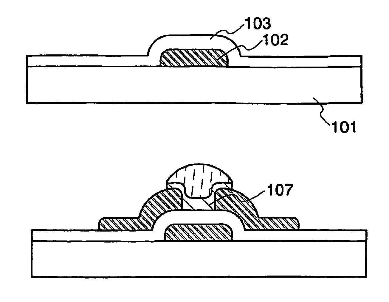
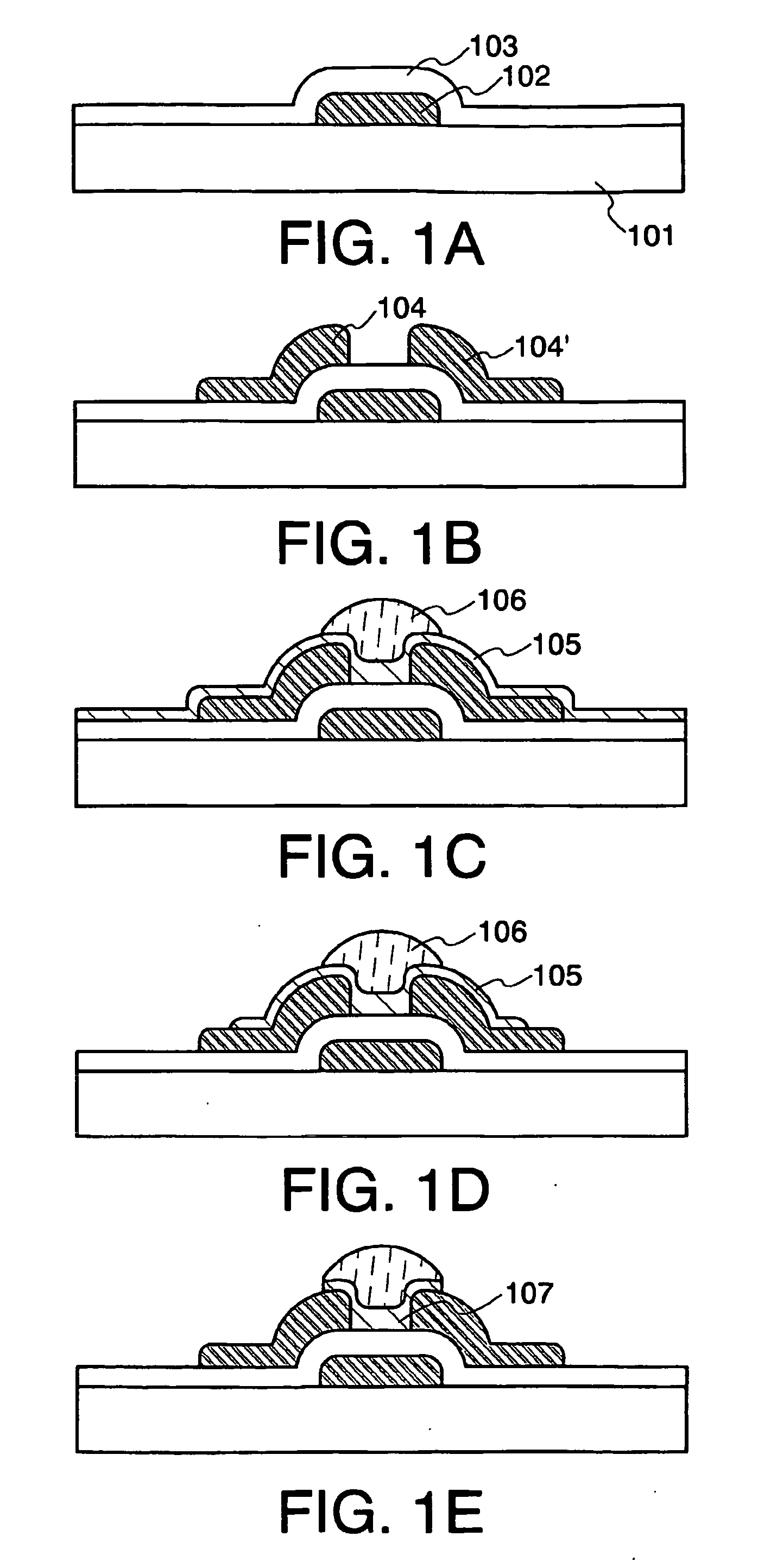
[0031] In this embodiment mode, a manufacturing method of an organic TFT according to the present invention is explained with reference to FIGS. IA to IE.

[0032] A substrate 101 having an insulating surface is prepared as shown in FIG. IA. A glass substrate, a quartz substrate, or a substrate formed from an insulating substance such as alumina can be used as this substrate 101. In addition, a substrate having flexibility may be used, and a substrate comprising one selected from polyethylene terephthalate (PET) polyethylenenaphthalate (PEN), polyethersulfone (PES), polycarbonate (PC), polyimide, and the like may be used.

[0033] Then, a gate electrode 102 of a TFT is formed over the substrate 101 using a material having conductivity by a droplet discharge method, a printing method, an electric field plating method, a PVD (Physical Vapor Deposition) method, a CVD (Chemical Vapor Deposition) method, a vapor deposition method, or the like. The film thickness of the gat...

embodiment mode 2

(Embodiment Mode 2)

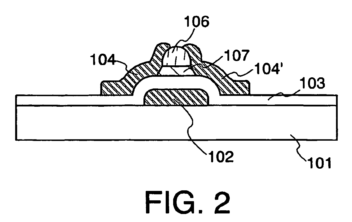
[0056] In this embodiment mode, a method for forming a top gate organic TFT is explained with reference to FIGS. 3A to 3D. In FIGS. 3A to 3D, as for the same reference numerals as in Embodiment Mode 1, the material, the forming method, and the like are referred to the description in Embodiment Mode 1.

[0057] Source and drain electrodes 104 and 104′ are formed over a substrate 101. Then, a semiconductor film 105 containing an organic material is formed over the substrate 101 and the source and drain electrodes, and then, a mask 106 is formed so as to be in contact with the semiconductor film 105 (FIGS. 3A and 3B).

[0058] Next, as shown in FIG. 3C, the semiconductor film 105 is patterned using the mask 106 to form a semiconductor layer 107. Subsequently, a gate electrode 102 is formed over the mask 106 in the state where the mask 106 is not removed to remain (FIG. 3D). In this embodiment mode, the mask 106 serves as both a protective film of the semiconductor layer ...

embodiment mode 3

(Embodiment Mode 3)

[0060] In this embodiment mode, a method for forming a first element which is an N type organic TFT and a second element which is a P type organic TFT simultaneously is explained with reference to FIGS. 4A to 4E. In FIGS. 4A to 4E, as for a substrate, a gate electrode, a gate insulating film, source and drain electrodes, a mask, a semiconductor film, a semiconductor layer, and the like having the same reference numerals as in Embodiment Mode 1, the material, the forming method, and the like thereof are referred to the description in Embodiment Mode 1.

[0061] A gate electrode 102a of a first element and a gate electrode 102b of a second element are formed over a substrate 101 in FIG. 4A. Then, a gate insulating film 103 is formed over the gate electrode 102a of the first element and the gate electrode 102b of the second element. Further, source and drain electrodes 104 and 104a′ of the first element, and source and drain electrodes 104b and 104b′ of the second elem...


PUM


Abstract

In view of the problem that an organic semiconductor layer of an organic TFT is likely to deteriorate due to water, light, oxygen, or the like, it is an object of the present invention to simplify a manufacturing step and to provide a method for manufacturing a semiconductor device having an organic TFT with high reliability. According to the invention, a semiconductor layer containing an organic material is formed by patterning using a mask, and thus an organic TFT is completed in the state where the mask is not removed but to remain over the semiconductor layer. In addition, a semiconductor layer can be protected from deterioration due to water, light, oxygen, or the like by using the remaining mask.

Description

TECHNICAL FIELD [0001] The present invention relates to a semiconductor device having an organic thin film transistor and a manufacturing method thereof. BACKGROUND ART [0002] Nowadays, a technique for making up a thin film transistor (TFT) with a semiconductor thin film (thickness of approximately from several nanometers to several hundred nanometers) formed over a substrate having an insulating surface attracts attention. A thin film transistor is widely applied to an electronic device such as an IC and an electro-optic device. In particular, a thin film transistor has been rushed to be developed as a switching element of a display device. [0003] The study of a thin film transistor using an organic semiconductor (hereinafter, referred to as “organic TFT”) among TFTs is proceeding. An organic TFT has good flexibility since an organic material is used. In addition, an organic TFT can be formed at lower temperature compared with a TFT using an inorganic semiconductor; therefore, a re...

Claims


Application Information

Patent Timeline
Patent Type & Authority Applications(United States)
IPC IPC(8): H01L51/40
CPCG02F1/1368H01L27/3274H01L51/10H01L51/0545H01L51/0018H10K59/125H10K71/233H10K10/80H10K10/466
Inventor MAEKAWA, SHINJI
Owner SEMICON ENERGY LAB CO LTD
Why Eureka
Try Eureka