Method for depositing thin film by controlling effective distance between showerhead and susceptor
Inactive Publication Date: 2007-02-08
ASM JAPAN
View PDF7 Cites 0 Cited by
Summary
Abstract
Description
Claims
Application Information
AI Technical Summary
This helps you quickly interpret patents by identifying the three key elements:
Problems solved by technology
Method used
Benefits of technology
Benefits of technology
[0008] The present invention has been achieved in view of these disadvantages. An object of the present invention is to provide a plasma CVD apparatus which can form a thin film having uniform film thickness and quality.
[0009] Another object of the present invention is to provide a plasma CVD apparatus with high process stability, a simple structure and low apparatus cost.
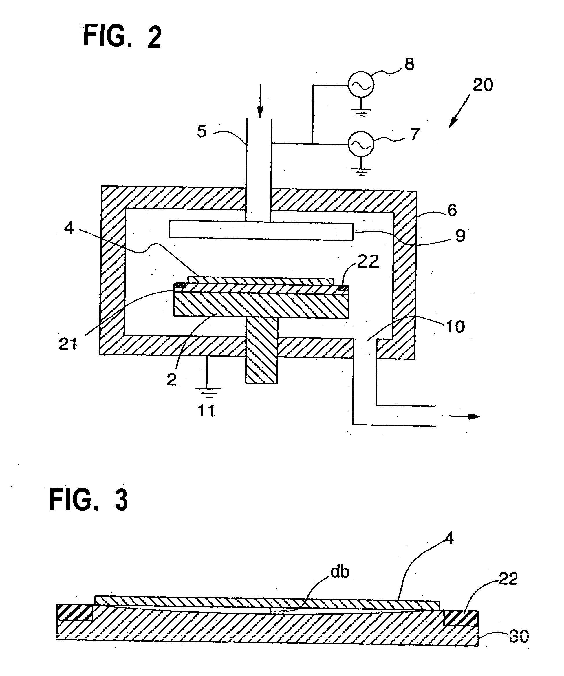
[0012] In the above, in an embodiment, the peripheral portion of the susceptor is a circularly formed recess to increase the electrically effective distance in the peripheral portion. In another embodiment, the peripheral portion of the susceptor is composed of a material having a lower dielectric constant than that of a material constituting the inner portion, to increase the electrically effective distance in the peripheral portion. In either case, the electrically effective distance between the showerhead and the susceptor is greater in the peripheral portion than in the inner portion, so that uniformity of a film can effectively be achieved without complicated operation control.
[0013] As described in the background section, the plasma density tends to be high at the center of the semiconductor wafer and low in an outer circumferential portion. Such a phenomenon can be explained based on the electric field intensity generated between the electrodes. According to the electric field intensity distribution, in order to increase the thickness of a film, the distance between the electrodes may need to be closer. However, to the contrary, in the present invention, by widening the distance between the electrodes in the vicinity of the periphery of the substrate, it is possible to effectively increase the thickness of a film near the periphery of a substrate, thereby forming a film having uniform thickness. This phenomenon may be explained based on (a) a residence time of a reaction gas and (b) a plasma density. That is, the wider the distance between the electrodes, the slower the flow rate of the reaction gas becomes, thereby increasing the deposition rate of a film. Further, the wider the distance between the electrodes, the higher the plasma density becomes, thereby increasing the deposition rate of a film.
Problems solved by technology
However, there were disadvantages in the conventional methods, including complicated operation and low process stability, because altering these parameters changes film quality and a deposition speed.
Method used
Image
Click on the blue label to locate the original text in one second.
Reading with bidirectional positioning of images and text.
Examples
examples
[0045] Experiments conducted for evaluating uniformity of a thickness of a low-k insulation film formed using the plasma CVD apparatus are described below.
experiment 1
[0046] Using the plasma CVD apparatus 20 shown in FIG. 2, an experiment for forming an insulation film on a Ø300 mm silicon wafer was conducted.
Experimental Conditions:
[0047] Main source gas: DM-DMOS (dimethy-dimethoxysilane) 200 sccm
[0048] Added gas: He 400 sccm
[0049] Primary radio-frequency power source: 27.12 MHz at 2.5 W / cm2
[0050] Secondary radio-frequency power source: 400 kHz at 0.1 W / cm2
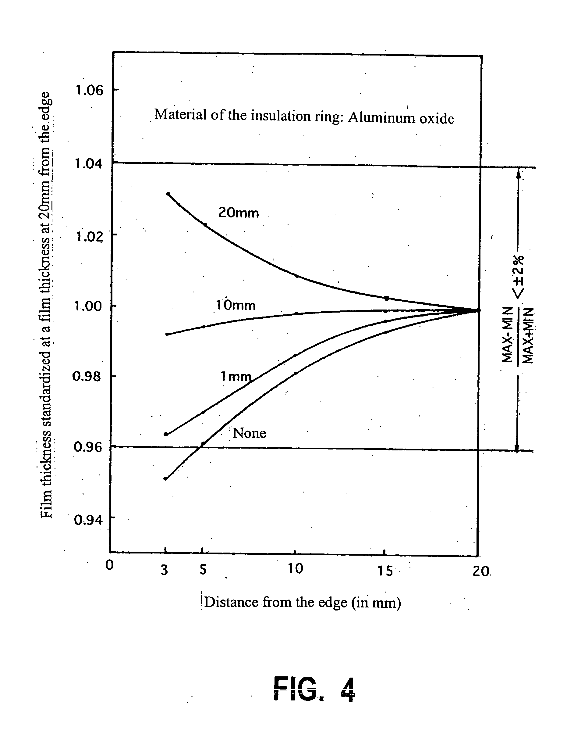
[0052] Material of the insulation ring: Aluminum oxide
[0053] Inner diameter of the insulation ring: 304 mm
[0054] Outer diameter of the insulation ring: 360 mm
[0055] Thickness of the insulation ring: 1 mm to 20 mm
[0056]FIG. 4 is a graph showing the relation between the distance from the edge of a semiconductor wafer and the film thickness standardized at 20 mm from the edge of the semiconductor wafer when the insulation film was formed on the semiconductor wafer under the above-mentioned experimental conditions. From the graph, it is seen that under...
experiment 2
[0057] Using the plasma CVD apparatus 20 shown in FIG. 2, an experiment for forming an insulation film on a Ø300 mm silicon wafer was conducted.
Experimental Conditions:
[0058] Main source gas: DM-DMOS (dimethy-dimethoxysilane) 200 sccm
[0059] Added gas: He 400 sccm
[0060] Primary radio-frequency power source: 27.12 MHz at 2.5 W / cm2
[0061] Secondary radio-frequency power source: 400 kHz at 0.1 W / cm2
[0063] Material of the insulation ring: Aluminum nitride
[0064] Inner diameter of the insulation ring: 304 mm
[0065] Outer diameter of the insulation ring: 360 mm
[0066] Thickness of the insulation ring: 1 mm to 20 mm
[0067]FIG. 5 is a graph showing the relation between the distance from the edge of a semiconductor wafer and the film thickness standardized at 20 mm from the edge of the semiconductor wafer when an insulation film was formed on the semiconductor wafer under the above-mentioned experimental conditions. From the graph, it is seen that unde...
PUM
Property
Measurement
Unit
Fraction
aaaaa
aaaaa
Thickness
aaaaa
aaaaa
Thickness
aaaaa
aaaaa
Abstract
A method for depositing a thin film on a substrate by plasma CVD includes: providing a vacuum chamber including a showerhead and a susceptor entirely facing the showerhead in parallel, placing a substrate on the susceptor entirely within the inner portion; and applying an RF power between the showerhead and the susceptor to deposit a thin film on the substrate. The susceptor includes an inner portion and a peripheral portion that is defined as any portion enclosing the inner portion and defines an electrically effective distance from the showerhead greater than that defined by the inner portion.
Description
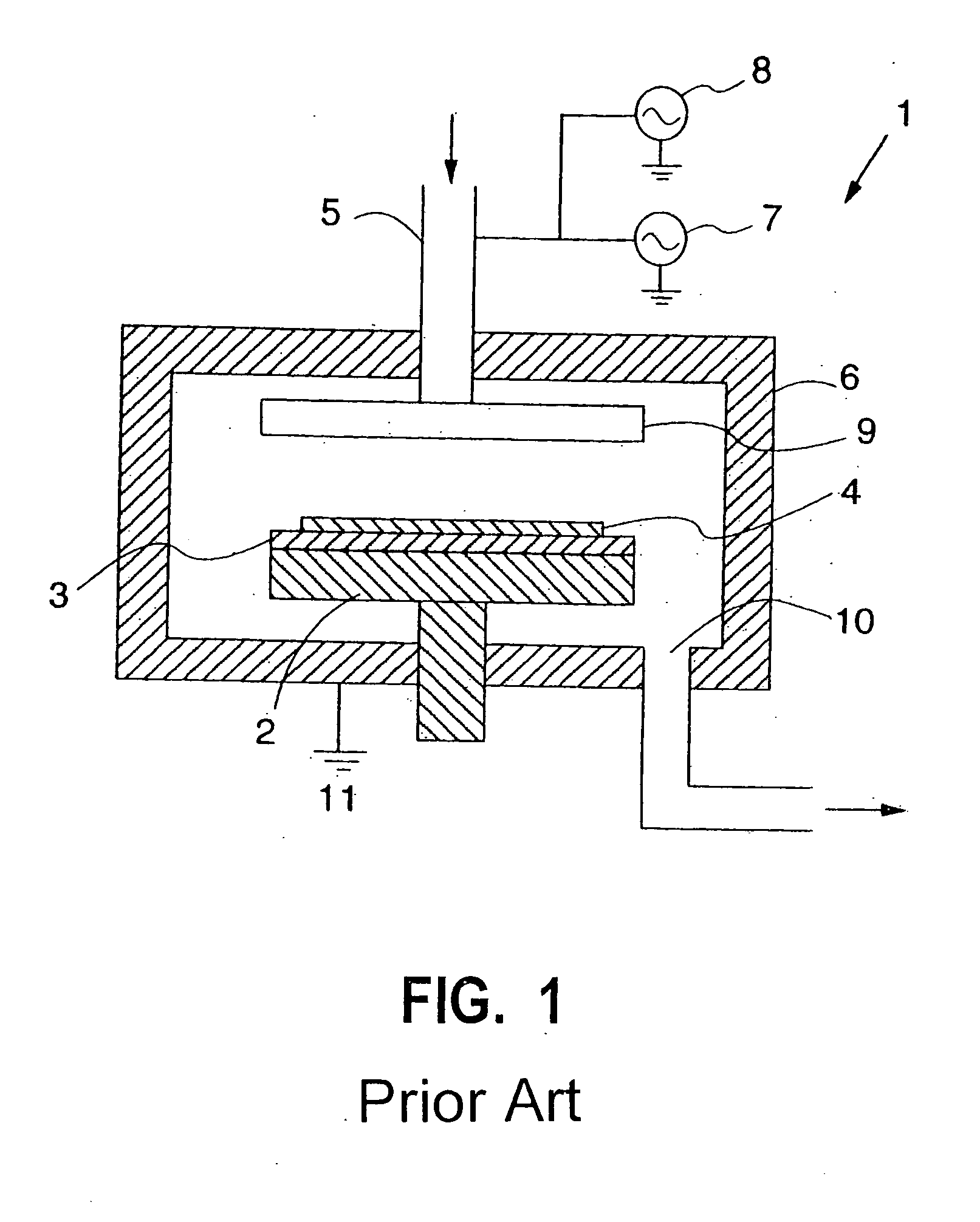
CROSS REFERENCE TO RELATED APPLICATIONS [0001] This is a continuation of U.S. patent application Ser. No. 10 / 412,822, filed Apr. 11, 2003, which claims priority to Japanese application No. 2002-112837, filed Apr. 16, 2002, and the disclosure of which is herein incorporated by reference in its entirety.BACKGROUND OF THE INVENTION [0002] 1. Field of the Invention [0003] The present invention relates to a plasma CVD apparatus for forming a thin film on a semiconductorwafer, and it particularly relates to a plasma CVD apparatus characterized by its susceptor structures. [0004] 2. Description of the Related Art [0005] In the past, plasma CVD has been used for forming a thin film on a workpiece to be processed such as a semiconductorwafer. FIG. 1 shows a schematic view of a conventional plasma CVD apparatus. The plasma CVD apparatus 1 includes a reaction chamber 6. Inside the reaction chamber 6, a susceptor 3 for placing thereon a semiconductorwafer 4 is disposed. The susceptor 3 is su...
Claims
Application Information
Patent Timeline
Application Date:The date an application was filed.
Publication Date:The date a patent or application was officially published.
First Publication Date:The earliest publication date of a patent with the same application number.
Issue Date:Publication date of the patent grant document.
PCT Entry Date:The Entry date of PCT National Phase.
Estimated Expiry Date:The statutory expiry date of a patent right according to the Patent Law, and it is the longest term of protection that the patent right can achieve without the termination of the patent right due to other reasons(Term extension factor has been taken into account ).
Invalid Date:Actual expiry date is based on effective date or publication date of legal transaction data of invalid patent.

