
Interconnect model-order reduction method

a technology of interconnects and models, applied in error detection/correction, program control, instruments, etc., can solve the problems of increasing the order of the corresponding interconnect models, the complexity of the circuit associated with the semiconductor device, and the difficulty of real application, so as to achieve rapid and accurate

Inactive Publication Date: 2007-02-08
CHANG GUNG UNIVERSITY
View PDF7 Cites 3 Cited by
  • Summary
  • Abstract
  • Description
  • Claims
  • Application Information

AI Technical Summary

Benefits of technology

[0008] It is, therefore, an object to provide an interconnect model-order reduction method for reduction of a nano-level semiconductor interconnect network as an original interconnect network into a reduced interconnect model for signal analysis by using iteration-based Arnoldi algorithm, through which transfer functions of the original interconnect network and the reduced interconnect model is exempted from complicated computations and the reduced interconnect model may be achieved in a rapid and accurate manner.
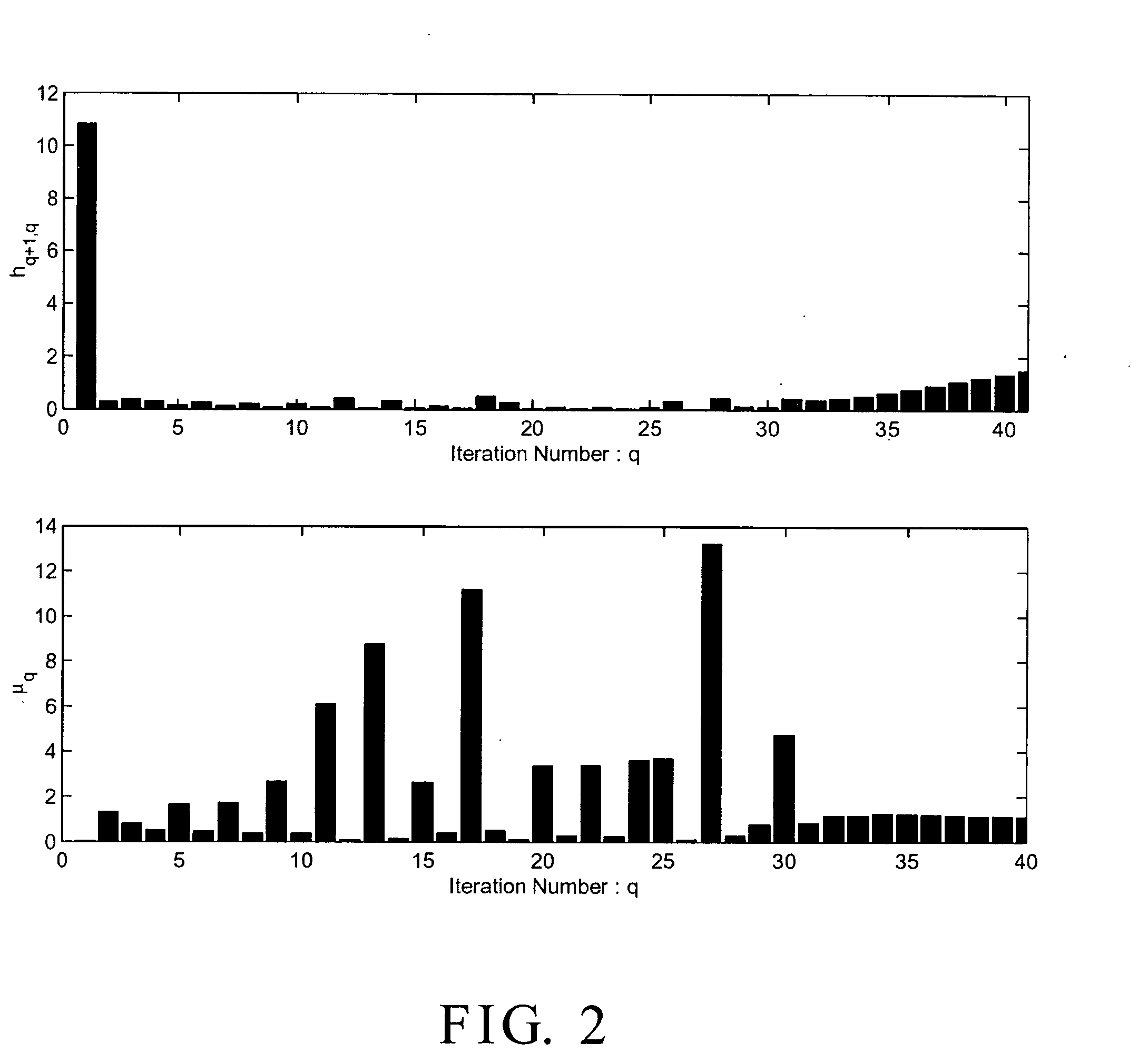
[0012] The thus derived error may efficiently provide a reference for order of the reduced interconnect model selected by Krylov subspace model reduction algorithm.

Problems solved by technology

Since complexity of circuit associated with the semiconductor device is increased, order of the corresponding interconnect model is also increased.
However, the error E(s) is involved with complicated computations of a resolvent matrix (In−sA)−1 of the original system, making itself difficult to be used in a real application.

Method used

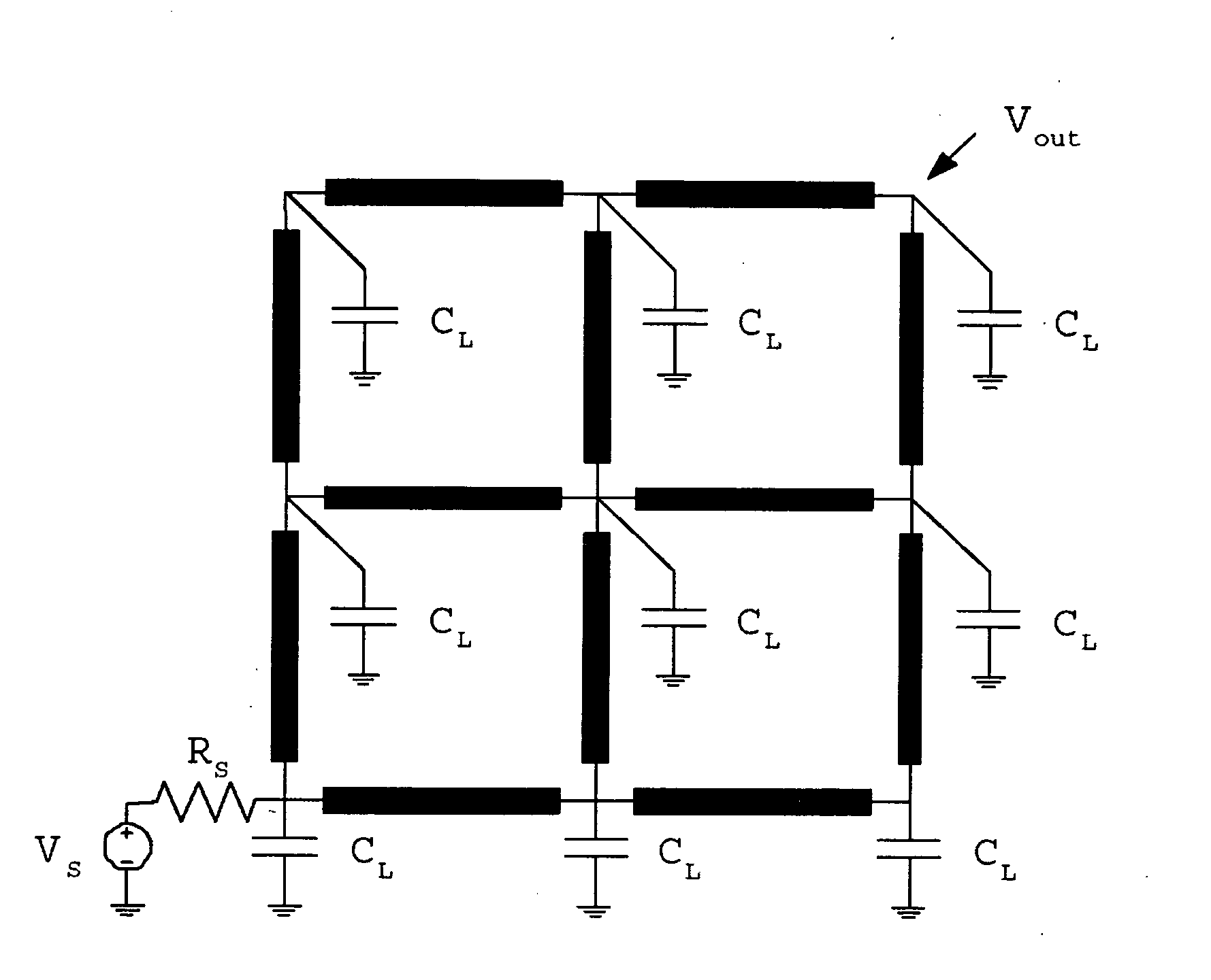

Image

  • Interconnect model-order reduction method
  • Interconnect model-order reduction method
  • Interconnect model-order reduction method

Examples


Embodiment Construction

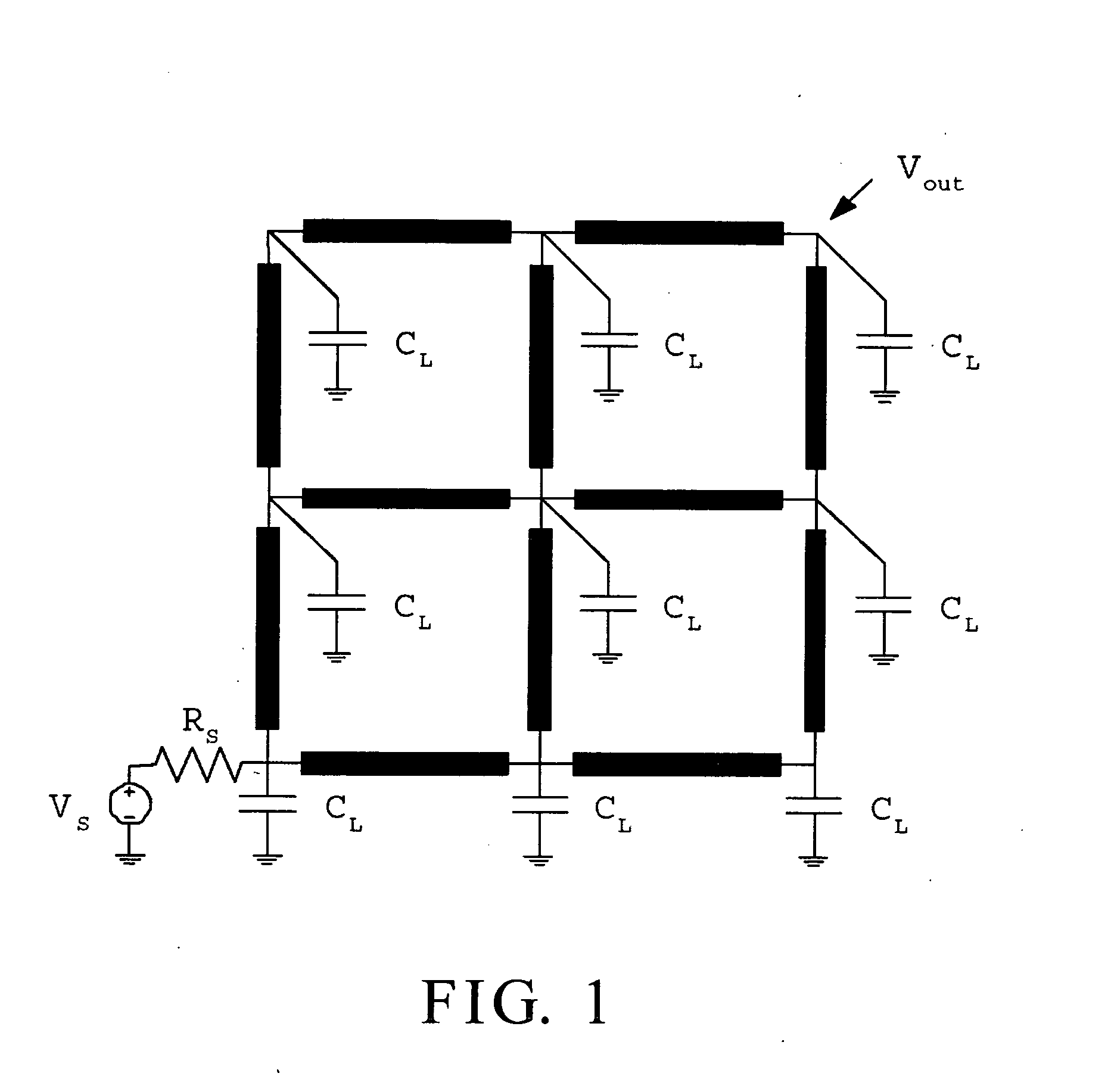
[0017] In analyzing a linear RLC interconnect network in an ultra-large semiconductor circuit (ULSI), modified nodal analysis (MNA) technology is generally utilized. In performing the MNA technology, the interconnect network may be first represented as the following state space-based equation: M⁢ⅆx⁡(t)ⅆt=-Nx⁡(t)+bu⁡(t),y⁡(t)=cT⁢x⁡(t),Eq. ⁢(1)

wherein M,N∈Rn×n,x,b,c∈Rn and y(t)∈R; and wherein M is a matrix including capacitances and inductances therein, N is a matrix including electric conductivities and resistances therein, x(t) is a state matrix including node voltages and branch currents of an inductor therein, u(t) is an input signal and y(t) is an output signal.

[0018] Now, assuming A=N−1M and r=N−1b, Eq. (1) may be represented as the following equation: A⁢ⅆx⁡(t)ⅆt=x⁡(t)-ru⁡(t),y⁡(t)=cT⁢x⁡(t).(Eq. ⁢2)

[0019] Now, the original interconnect network is to be reduced so as to obtain a reduced interconnect network so that essential dynamics of the original interconnect network may b...


PUM


Abstract

An interconnect model-order reduction method for reduction of a nano-level semiconductor interconnect network as an original interconnect network by using iteration-based Arnoldi algorithms disclosed. The method is performed based on a projection method and has become a necessity for efficient interconnect modeling and simulations. To select order of the reduced-order model that can efficiently reflect essential dynamics of the original interconnect network, a residual error between transfer functions of the original interconnect network and the reduced interconnect model may be considered as a reference in determining if the iteration process should end, analytical expressions of the residual error being derived herein. Furthermore, the approximate transfer function of the reduced interconnect model may also be expressed as an addition of the original interconnect model and some additive perturbations. A perturbation matrix is only related with resultant vectors at a previous step of the Arnoldi algorithm. Therefore, the residual error information may be taken as a reference for the order selection scheme used in Krylov subspace model-order algorithm.

Description

BACKGROUND OF THE INVENTION [0001] 1. Field of Invention [0002] The present invention relates to an interconnect model-order reduction method. More particularly, the present invention relates to a rapid and accurate interconnect model-order reduction method for reduction of a nano-level semiconductor interconnect network for signal analysis. [0003] 2. Related Art [0004] Complemented metal oxide semiconductor (CMOS) technology has heretofore advanced to be measured at nano-level and thus parasitic effect to interconnects of the related semiconductor device becomes inneglectable. Since complexity of circuit associated with the semiconductor device is increased, order of the corresponding interconnect model is also increased. Consequently, an efficient interconnect model-order reduction has become a necessity of modeling and simulation of the interconnect network. Such methods may be referred to in, for example, U.S. Pat. No. 6,023,573, U.S. Pat. No. 6,041,170 and U.S. Pat. No. 6,687,6...

Claims


Application Information

Patent Timeline
Patent Type & Authority Applications(United States)
IPC IPC(8): G06F17/50
CPCG06F17/5036G06F30/367
Inventor CHU, CHIA-CHILEE, HERNG-JERFENG, WU-SHIUNGCHANG, CHAO-KAI
Owner CHANG GUNG UNIVERSITY
Learn More