Photonic crystal emitter, detector and sensor

a technology of emitters and crystals, applied in the field of micro-machined devices, can solve the problems of reduced optical energy received by the detector, complex sensors, and high cost, and achieve the effect of high stability

Inactive Publication Date: 2007-02-15
FLIR SURVEILLANCE
View PDF21 Cites 58 Cited by
  • Summary
  • Abstract
  • Description
  • Claims
  • Application Information

AI Technical Summary

Benefits of technology

[0013] The infrared emitter utilizes a photonic bandgap (PBG) structure to produce electromagnetic emissions with a narrow band of wavelengths. A PBG structure is an artificially engineered periodic dielectric array in which the propagation of electromagnetic waves is governed by band structure-like dispersion. The structure exhibits allowed and forbidden propagation of electronic energy bands. The absence of allowed propagating electromagnetic wave modes inside the structures, in a range of wavelengths called a photonic band gap, gives rise to distinct optical phenomena such as inhibition of spontaneous emission, high-reflecting omnidirectional mirrors, low-loss-waveguides, etc.
[0014] According to one preferred embodiment, the emitter includes a semiconductor material layer, a dielectric material layer overlaying the semiconductor material layer, and an electrically conductive material layer having an inner side overlaying the dielectric material layer. Preferably, the semiconductor material layer is made from single-crystal silicon carbide (SiC), polycrystalline silicon carbide (poly-SiC), germanium, or the group III-V semiconductors, the group II-VI semiconductors including alloys of indium, gallium, aluminum, arsenic, antimony, and phosphorous, and alloys of zinc, mercury, cadmium, tellurium, sulphur and selenium. SiC exhibits a high stability at high temperatures, which makes SiC a good candidate for the emitter devices according to the present invention, especially for the devices that operate in a high temperature environment. The semiconductor material layer may be doped with N type or P type impurities. The dielectric material layer is preferably made from silicon dioxide, although other dielectric materials may be used. According to one aspect of the present invention, the dielectric material layer is selected from the group consisting of silicon nitride, alumina, sapphire, aluminum nitride, and silicon oxinitride. The electrically conductive material layer can be made from a metallic material or metallic-like material. The metallic material is preferably selected from but not limited to a group consisting of gold, aluminum, nickel, silver, titanium, and platinum, or an alloy of the above metals. The metallic-like material refers to a heavily doped semiconductor or a conductive ceramic selected from the group consisting of titanium nitride, tantalum nitride and indium tin oxide or other non-metal electrically conductive materials. The titanium nitride material allows conventional CMOS fabrication techniques to be used in the fabrication of the device according to the present invention. The electrically conductive material layer hereinafter is referred to as a metal or metallic-like material layer. Thus, the metallic-like layer can be a highly doped semiconductor with effective metallic properties or a conductive ceramic preferably made from but not limited to a group consisting of titanium nitride, tantalum nitride, and indium tin oxide. The semiconductor material layer is capable of being coupled to an energy source for introducing energy to the semiconductor material layer. The metallic material layer includes periodically distributed surface features on an outer side thereof opposite the inner side. The three material layers are adapted to transfer energy from the semiconductor material layer to the outer side of the metallic material layer and emit electromagnetic energy in a narrow band of wavelengths from the outer side of the metallic material layer. The device may have more than three or less than three layers of materials. The multi-layer structure emits electromagnetic waves with narrow peak wavelengths based on their resonances.
[0015] In one preferred form, the emitted electromagnetic energy has wavelengths centered about a characteristic wavelength (λ) and having a full width at half maximum (Δλ), where Δλ / λ is equal to or less than 0.5

Problems solved by technology

Thus, when the targeted gas is present in the optical path between the emitter and the detector, the optical energy received by the detector is reduced, and the temperature of the detector drops, which in turn results in changing of the resistance of the detector.
Furthermore, the sensors constructed as described above are multi-component systems requiring special alignment, calibration, and separate electronics for both the emitter and the detector making this sensors complex and expensive.
While this technique is highly sensitive and less subject to contamination and false alarms than electrochemical sensors, the units are expensive for home installation.
In addition, because they depend on physical band-gaps, diode lasers can only be tuned with difficulty within a very narrow range.
However, the devices disclosed in the U.S. Pat. No. 6,756,594 are not suitable for very-high-temperature applications.

Method used


Image

  • Photonic crystal emitter, detector and sensor
  • Photonic crystal emitter, detector and sensor
  • Photonic crystal emitter, detector and sensor

Examples


example i

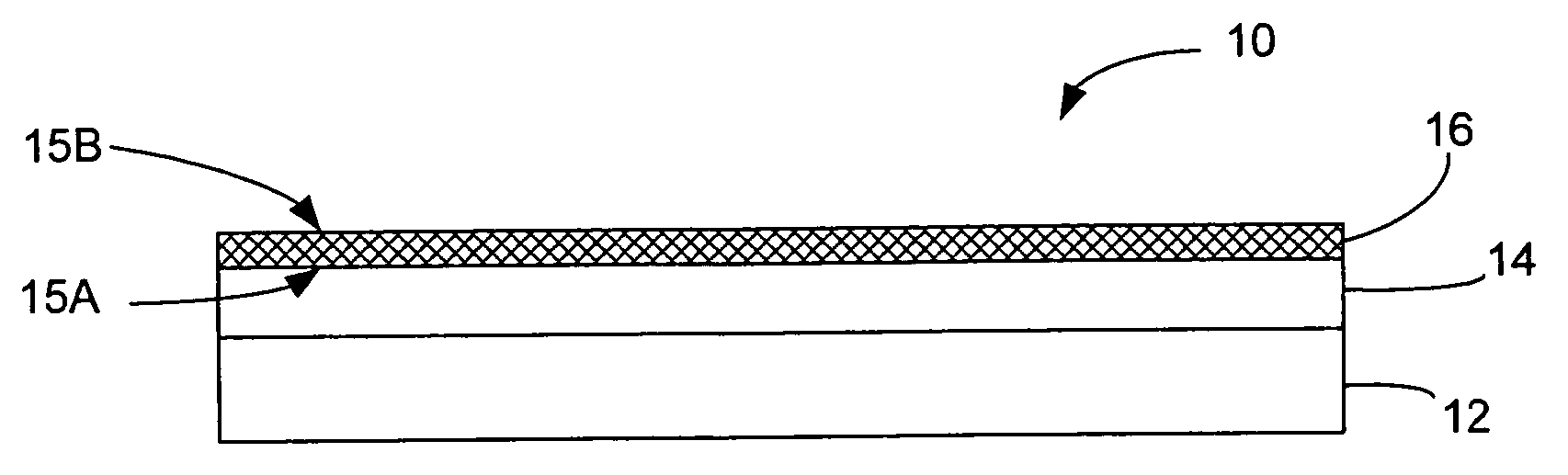
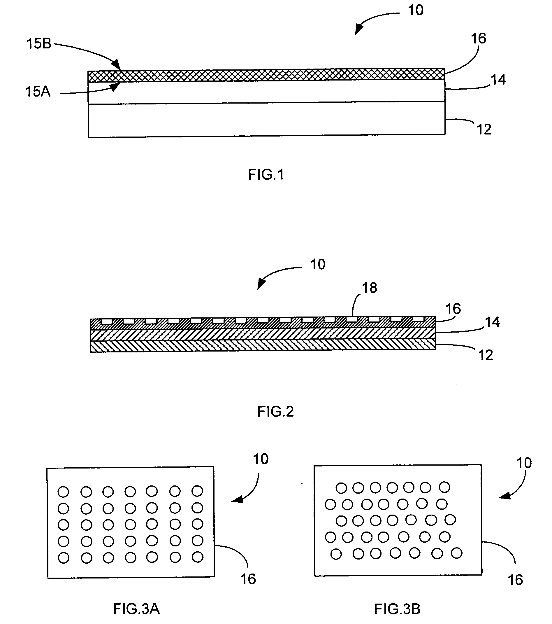
[0088] An infrared gas sensor embodying the present invention is schematically shown in FIG. 14. The infrared gas sensor utilizes a heated bolometer element, which employs a photonic bandgap structure, as both the source and the detector in an open path atmospheric gas measurement. The heated bolometer is a MEMS device as denoted by number 500, which is a thin silicon membrane with a gold coating. A repetitive pattern of holes are etched into the emitter surface. The repetitive pattern forms the 2-D photonic bandgap structure on the top surface of the MEMS device. The MEMS device is heated by passing an electrical current through the silicon layer, and the 2-D photonic bandgap coating emits a narrow line spectrum. The MEMS device also has particularly high absorption for the same wavelength it emits. The MEMS device 500 is placed opposite a mirror 502. In the absence of the monitored species (that absorb the electromagnetic energy at the emitted spectrum), the bolometer reaches radi...

example ii

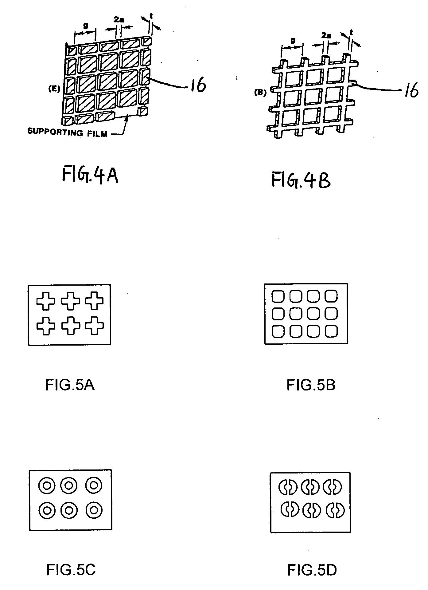
[0089] An emitter device including a SiC layer coated with platinum is fabricated. FIG. 16A shows a top view of the device and FIG. 16B shows a side cross-sectional view. As seen in FIG. 16A, circular holes are etched into the SiC layer. The holes are distributed in a two-dimentional parallelogram lattice geometry. The diameter and the inter-spacing of the holes is about 2.5 μm. The depth of the holes is about 2 μm. The thickness of the platinum layer is less than 1 μm. As seen in the figures, the resulted holes may not be perfect circles. The metal recesses from the edge of some of the holes. The resulted device, upon heated by electrical current conducted to the SiC layer, emits / absorbs infrared light in a narrow wavelength band. Different embodiments with different inter-hole spacing are manufactured and tested. The peak wavelengths of the emissions are plotted as a function of the inter-hole spacing. As shown in FIG. 17, the peak wavelength of the emissions is proportional to th...


PUM


Abstract

An infrared emitter, which utilizes a photonic bandgap (PBG) structure to produce electromagnetic emissions with a narrow band of wavelengths, includes a semiconductor material layer, a dielectric material layer overlaying the semiconductor material layer, and a metallic material layer having an inner side overlaying the dielectric material layer. The semiconductor material layer is capable of being coupled to an energy source for introducing energy to the semiconductor material layer. An array of holes are defined in the device in a periodic manner, wherein each hole extends at least partially through the metallic material layer. The three material layers are adapted to transfer energy from the semiconductor material layer to the outer side of the metallic material layer and emit electromagnetic energy in a narrow band of wavelengths from the outer side of the metallic material layer.

Description

CROSS-REFERENCE TO RELATED APPLICATION [0001] The present application claims priority to provisional U.S. patent application Ser. No. 60 / 580,574, filed Jun. 17, 2004, and provisional U.S. patent application Ser. No. 60 / 586,334, filed Jul. 8, 2004, the disclosures of which are incorporated herein by reference.FIELD OF THE INVENTION [0002] The present invention relates to infrared emitters / detectors / sensors for emitting and / or detecting infrared electromagnetic energy, and more particularly, to micromachined devices for emitting and / or detecting infrared electromagnetic waves. BACKGROUND OF THE INVENTION [0003] Infrared emitters / detectors / sensors are used in many applications, for example, in detecting and discriminating the presence of specific biological, chemical substances (e.g., gases). [0004] A conventional detector or sensor typically includes a heated element as a source of infrared emission, a filter for controlling the wavelength of emitted light, and a detector for detectin...

Claims


Application Information

Patent Timeline
Patent Type & Authority Applications(United States)
IPC IPC(8): H01L31/0232
CPCB82Y20/00H01L27/14676G01J1/0252G01J1/42G01J3/02G01J3/0286G01J3/108G01J5/02G01J5/023G01J5/024G01J5/04G01J5/045G01J5/046G01J5/08G01J5/0803G01J5/0853G01J5/0862G01J5/20G01N21/3504G01N2021/317G01N2021/3513G02B6/1225G01J1/02G01J5/0802
Inventor PRALLE, MARTIN U.DALY, JAMES T.PUSCASU, IRINAMCNEAL, MARK P.JOHNSON, EDWARD A.
Owner FLIR SURVEILLANCE
Why Eureka
Try Eureka