Method for fabricating semiconductor device and semiconductor device
- Summary
- Abstract
- Description
- Claims
- Application Information
AI Technical Summary
Benefits of technology
Problems solved by technology
Method used
Image

Examples
embodiment 1
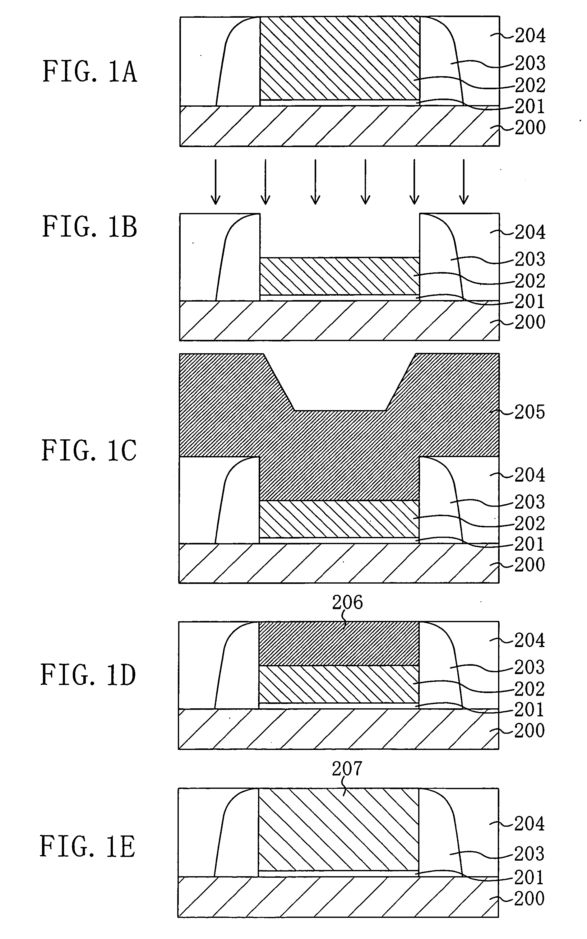
[0025] Hereinafter, a method for fabricating a semiconductor device according to a first embodiment of the present invention will be described with reference to the drawings.
[0026]FIGS. 1A through 1E are cross-sectional views showing a method for fabricating a semiconductor device according to the first embodiment.
[0027] First, as illustrated in FIG. 1A, a SiON film with a thickness of 2 nm and a polysilicon layer with a thickness of 100 nm are deposited over a semiconductor substrate 200 made of, for example, silicon (Si). Then, the SiON film and the polysilicon layer are partially etched, thereby forming a gate insulating film 201 with a thickness of about 2 nm and a silicon gate 202 with a thickness of 100 nm and a gate length of about 100 nm. Thereafter, extension implantation is performed using the silicon gate 202 as a mask, and then sidewalls 203 made of an insulating film and having a height of 100 nm are formed on side faces of the gate insulating film 201 and the silicon...
modified example of embodiment 1
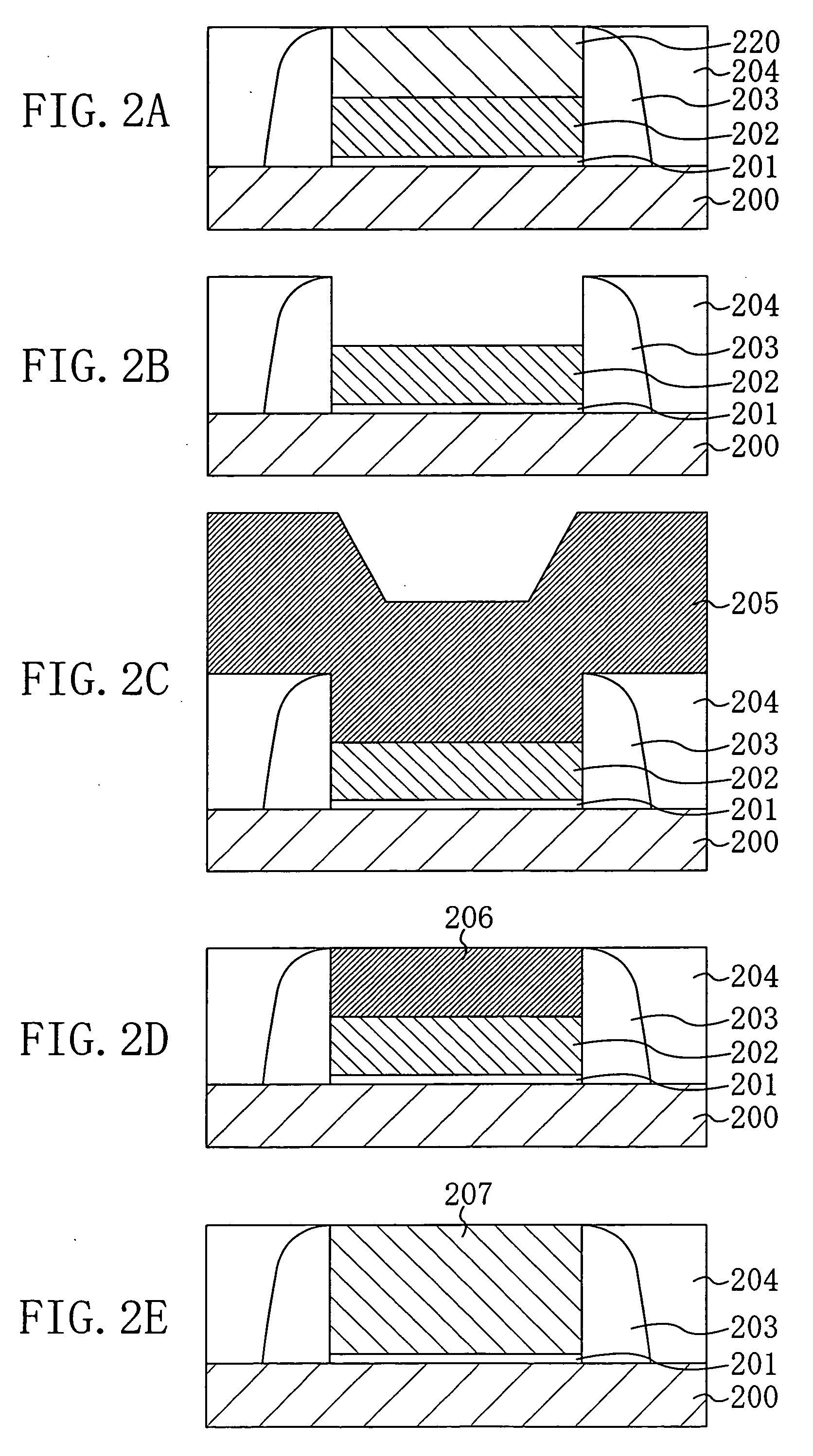
[0039]FIGS. 2A through 2E are cross-sectional views showing a method for fabricating a semiconductor device according to a modified example of the first embodiment. This modified example is different from the first embodiment in process steps up to the formation of the silicon gate 202.
[0040] First, as illustrated in FIG. 2A, a SiON film with a thickness of 2 nm and a polysilicon layer with a thickness of 50 nm are deposited over a semiconductor substrate 200. Then, a phospho-silicate glass (PSG) layer with a thickness of 50 nm is formed on the polysilicon layer. Thereafter, the PSG layer, the polysilicon layer and the SiON film are partially etched, thereby forming a gate insulating film 201 with a thickness of 2 nm, a silicon gate 202 with a thickness of 50 nm and a protective layer 220 with a thickness of 50 nm, respectively. Subsequently, extension implantation is performed using the silicon gate 202 and the protective layer 220 as masks. Then, sidewalls 203 of an insulating fi...
embodiment 2
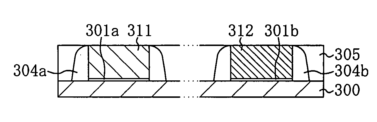
[0044] Hereinafter, a method for fabricating a semiconductor device according to a second embodiment of the present invention will be described with reference to the drawings. FIGS. 3A through 3H are cross-sectional views showing a method for fabricating a semiconductor device according to the second embodiment. The method of this embodiment is directed to a method for fabricating a MIS transistor including FUSI gate electrodes having different silicide phases on a wafer. In this embodiment, a NiSi phase is used for a gate electrode of an n-channel MIS (nMIS) transistor and a Ni3Si phase is used for a gate electrode of a p-channel MIS (pMIS) transistor. In each of FIGS. 3A through 3H, an nMIS region is shown in the left side and a pMIS region is shown in the right side.
[0045] First, as illustrated in FIG. 3A, in the same manner as in the first embodiment, a first gate insulating film 301a, a first silicon gate 302 of polysilicon, first sidewalls 304a and source / drain regions (not s...
PUM
 Abstract
Description
Claims
Application Information
PatSnap Eureka turns technology decisions into work you can execute. Powered by our Innovation Knowledge Graph, it runs expert workflows across engineering, life sciences, materials and intellectual property. Get your review-ready output in minutes.


