
Plasma display panel and method of manufacturing the same

Inactive Publication Date: 2007-03-01
SAMSUNG SDI CO LTD
View PDF28 Cites 8 Cited by
  • Summary
  • Abstract
  • Description
  • Claims
  • Application Information

AI Technical Summary

Benefits of technology

[0019] The present embodiments provide a plasma display panel having an improved exhaust structure to increase the gas exhaust capability of the plasma display panel, and a method of manufacturing the same.
[0020] In one aspect of the present embodiments, the space efficiency of the discharge cells of a PDP can be increased by disposing a plurality of electrodes around the discharge cells. In some embodiments, an improved exhaust structure for gas exhaustion is also included.

Problems solved by technology

Therefore, a high efficiency flat panel display device cannot be realized.
Second, when a conventional panel is operated for a prolonged period of time, a permanent latent image occurs due to ion sputtering of charged particles of a discharge gas onto a phosphor layer due to an electric field produced when the discharge diffuses toward the phosphor layer.
At this time, the discharge diffuses along the plane of the first substrate, and thus the space efficiency of the discharge cells is low.
However, the high concentration of the Xe gas results in a high initial discharge firing voltage.

Method used


Image

  • Plasma display panel and method of manufacturing the same
  • Plasma display panel and method of manufacturing the same
  • Plasma display panel and method of manufacturing the same

Examples


Embodiment Construction

[0034] The present embodiments will now be described more fully with reference to the accompanying drawings in which exemplary embodiments are shown.

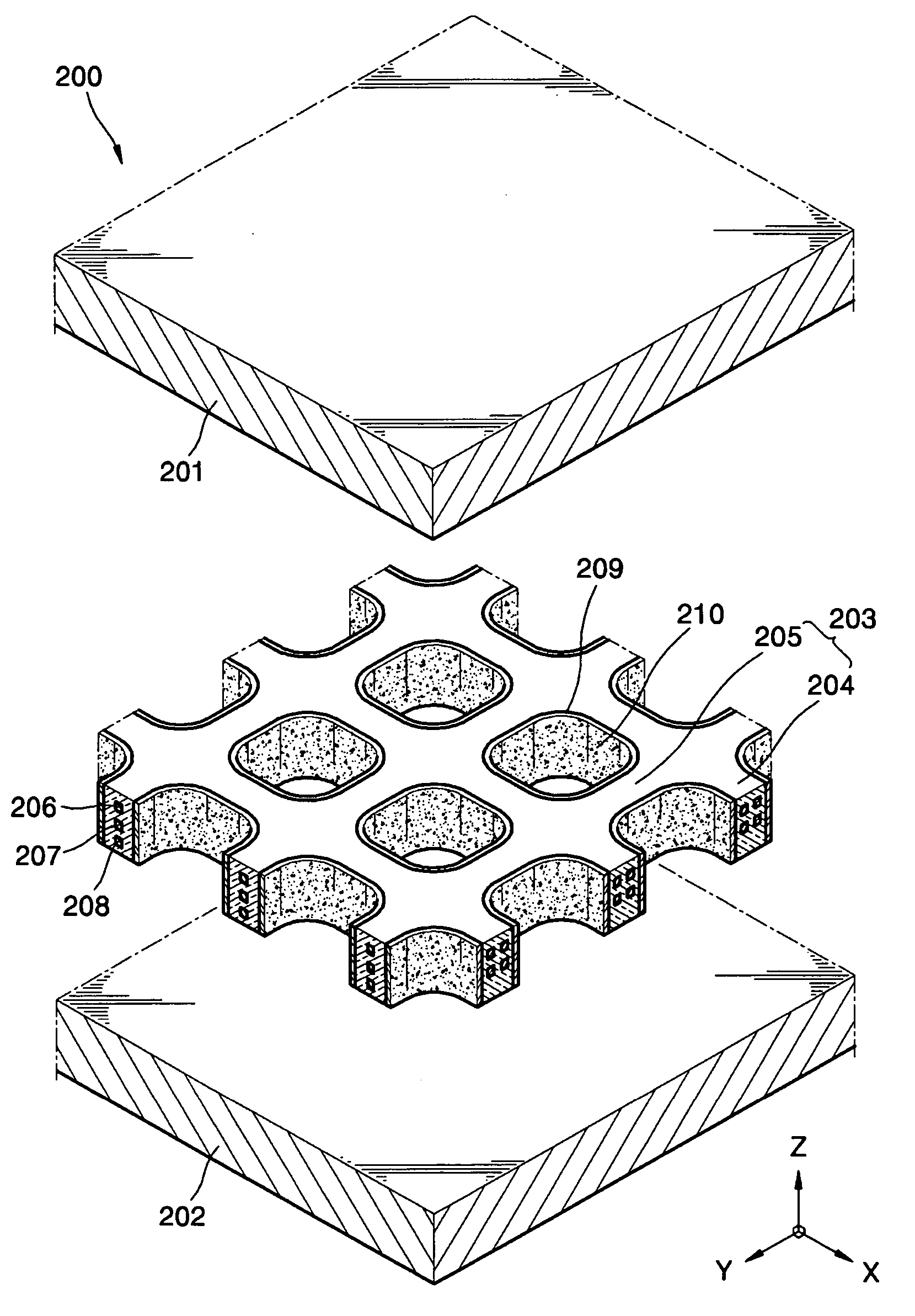
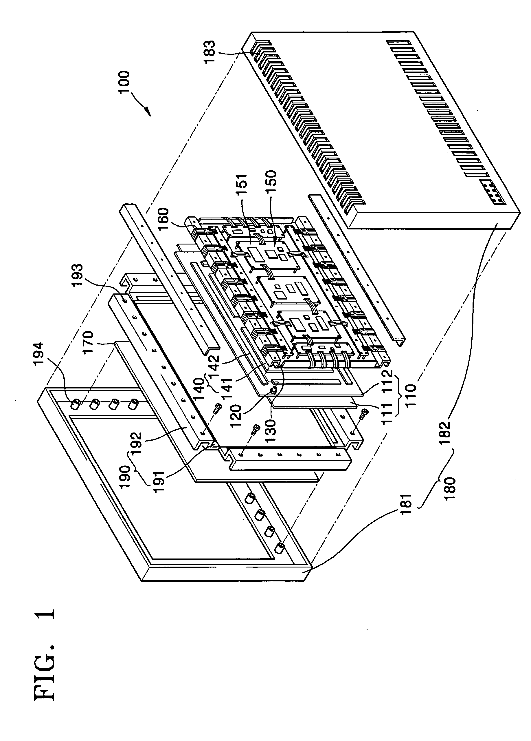
[0035]FIG. 1 is an exploded perspective view of a plasma display device assembly 100 according to an embodiment.

[0036] Referring to FIG. 1, the plasma display device assembly 100 includes a panel assembly 110 having a front panel 111, which is a first panel, and a rear panel 112, which is a second panel, facing the front panel 111. An inner space between the front panel 111 and the rear panel 112 is sealed from the outside by coating a sealing member such as frit glass, which will be described later, along inner edges of the front panel 111 and the rear panel 112 facing each other.

[0037] Also, an exhaust pipe 120 for discharging an exhaust gas containing impurity gases from a discharge space of the panel assembly 110 during a vacuuming process is installed on an outer edge of the rear panel 112.

[0038] A chassis base 130 is disposed ...


PUM


Abstract

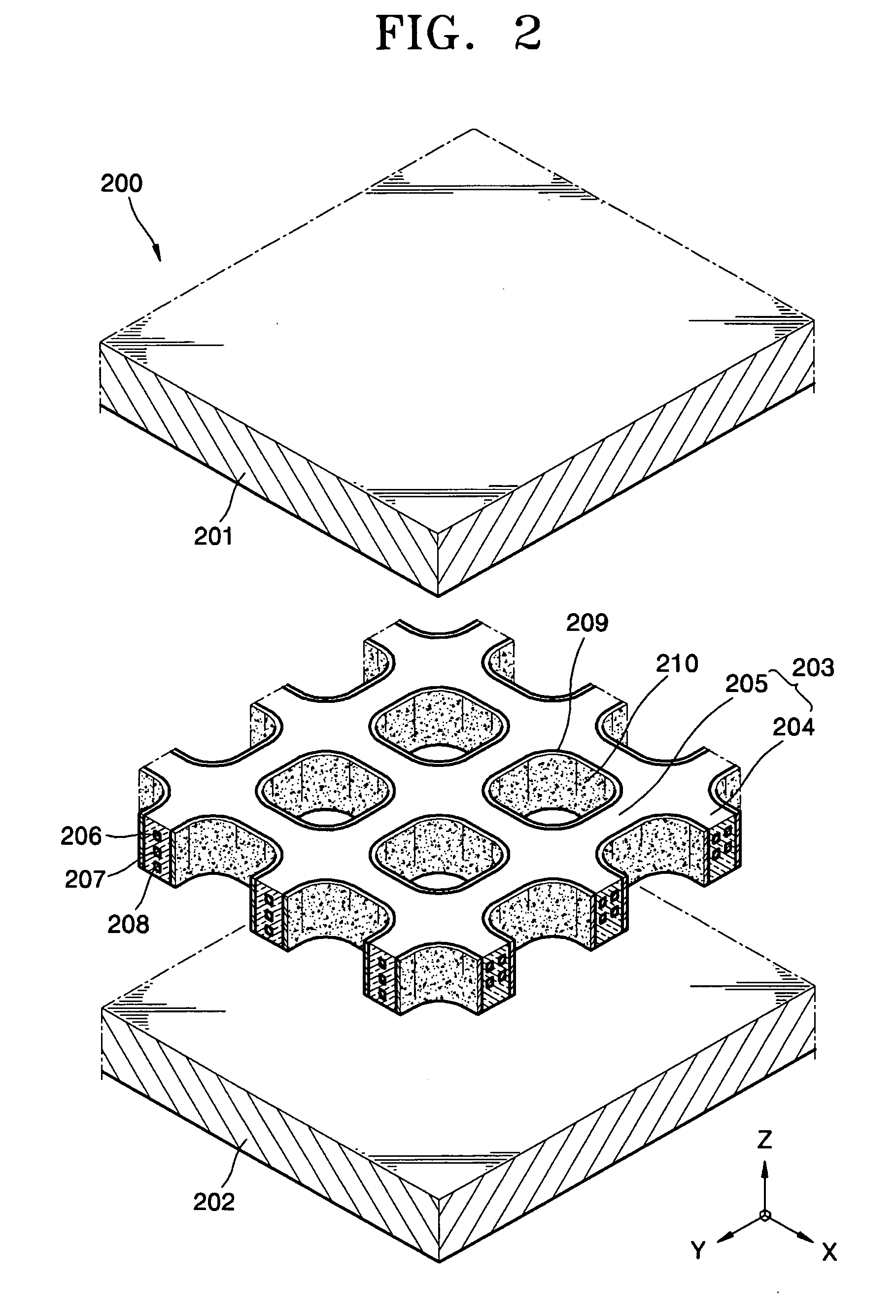
Provided is a plasma display panel and a method of manufacturing the same. The method of manufacturing the plasma display panel includes preparing a front substrate and a rear substrate and arranging the front and rear substrates to face each other; forming an exhaust hole in a discharge sheet; disposing the discharge sheet between the front and rear substrates; sealing a space between the front and rear substrates by coating a sealing member along edge surfaces of the front and rear substrates; and vacuuming the space between the front and rear substrates through an exhaust pipe formed on an outer surface of one of the front and rear substrates and connected to the exhaust pipe. The exhaust hole formed between the substrates has greater diameter than the discharge cells defined by the dielectric walls. Therefore, an inner region of the front substrate and an inner region of the rear substrate are subjected to substantially the same force.

Description

CROSS-REFERENCE TO RELATED APPLICATIONS [0001] This application claims the benefit of Korean Patent Application No. 10-2005-0079122, filed on Aug. 27, 2005, in the Korean Intellectual Property Office, the disclosure of which is incorporated herein in its entirety by reference. BACKGROUND OF THE INVENTION [0002] 1. Field of the Invention [0003] The present embodiments relate to a plasma display panel, and more particularly, to a plasma display panel having an improved exhaust hole structure so that air can be smoothly exhausted when the plasma display panel is vacuumed, and a method of manufacturing the same. [0004] 2. Description of the Related Art [0005] Generally, plasma display panels (PDPs) can be classified into direct current (DC) PDPs and alternating current (AC) PDPs according to the type of driving voltage applied to discharge cells, i.e., according to discharge type. PDPs can further be classified into facing discharge PDPs and surface discharge PDPs according to the arran...

Claims


Application Information

Patent Timeline
IPC IPC(8): H01J17/49
CPCH01J11/54H01J11/16H01J9/385H01J11/32H01J11/36H01J11/40H01J2211/323H01J2211/365
Inventor KWON, JAE-IKYI, WON-JUAHN, HO-YOUNGKANG, KYOUNG-DOOPARK, SOO-HOWOO, SEOK-GYUN
Owner SAMSUNG SDI CO LTD
Learn More