Semiconductor device and its manufacture method
a semiconductor and manufacturing method technology, applied in semiconductor devices, semiconductor/solid-state device details, electrical devices, etc., can solve the problems of insufficient tight adhesion of state before heat treatment, difficult to fill wiring trenches and via holes with copper at good reproductivity, etc., to prevent copper wiring from being peeled off, good reproductivity, and sufficient tight adhesion of wiring material
- Summary
- Abstract
- Description
- Claims
- Application Information
AI Technical Summary
Benefits of technology
Problems solved by technology
Method used
Image

Examples
first embodiment
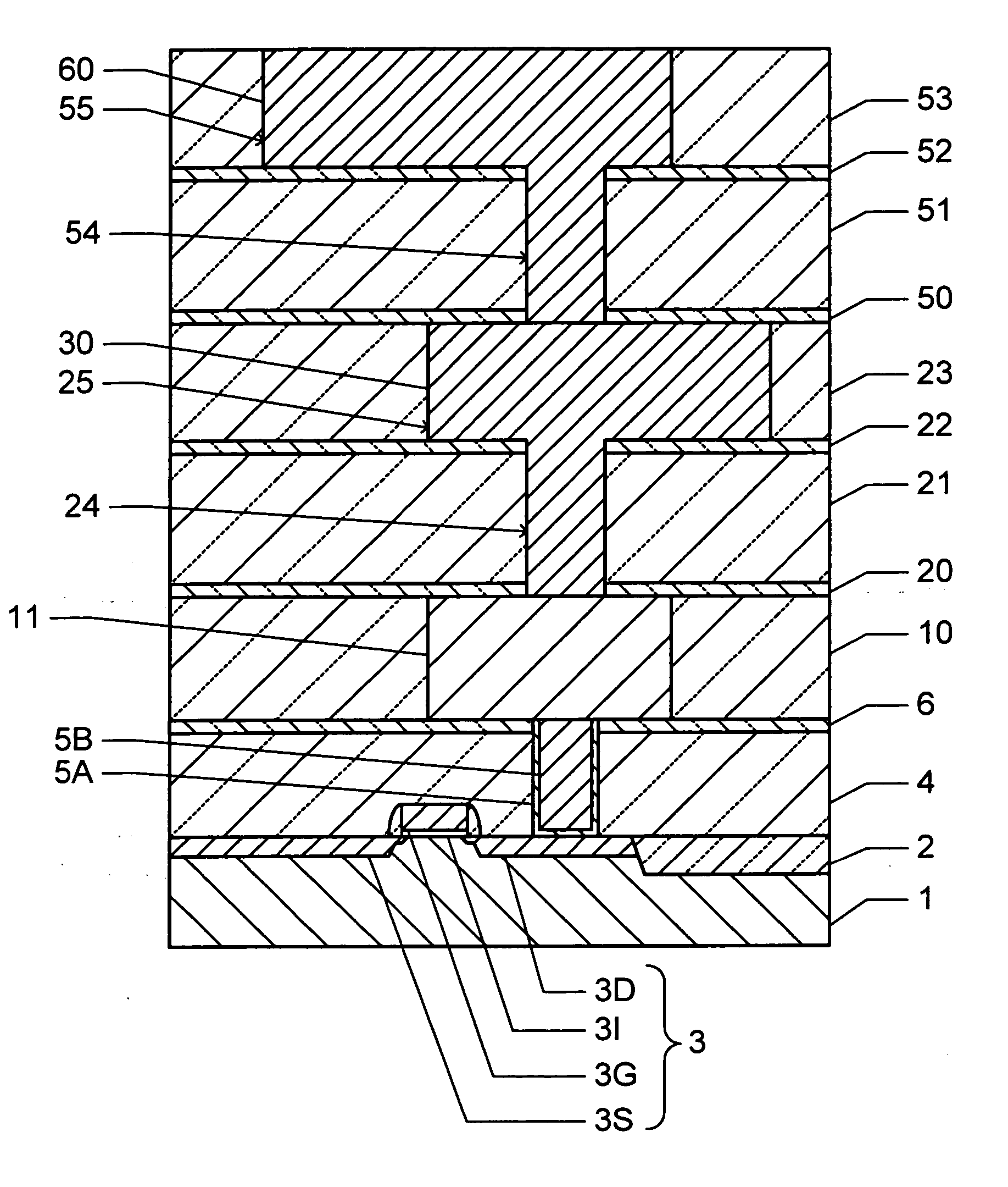
[0038] With reference to FIGS. 3A to 3F, description will be made on a semiconductor device manufacture method according to the In the following description, attention is paid to a method of forming the second layer wiring structure from the cap layer 20 to interlayer insulating film 23. The second layer wiring structure is formed by a dual damascene method. The third layer wiring structure is formed by the same method as that used for the second layer wiring structure. The first layer wiring 11 is formed by a single damascene method, and a barrier layer forming method, a method of depositing a conductive member in the wiring trench are the same as those adopted in the method of forming the second layer wiring structure.
[0039] As shown in FIG. 3A, a cap film 20, a via interlayer insulating film 21, an etching stopper film 22 and a wiring interlayer insulating film 23 are sequentially formed on an interlayer insulating film 10. For example, the cap film 20 has a two-layer structure ...
second embodiment
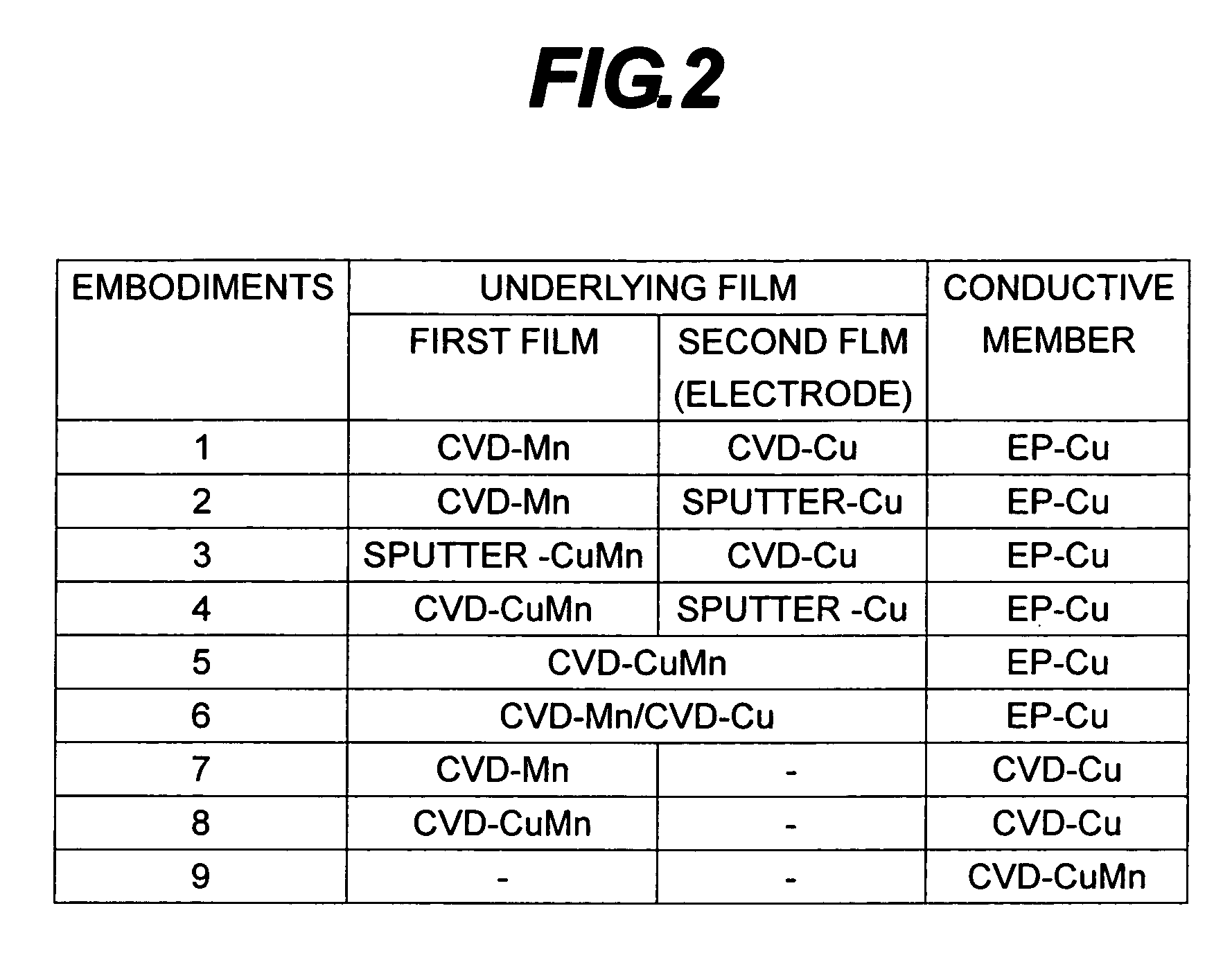
[0057] Since a method of forming a Cu film by sputtering is already use in a mass production, the method has excellent process stability. Also in the second embodiment, since the first film 32 is formed by CVD, sufficient adhesion can be ensured between the first film 32 and underlying insulating film.
[0058] Next, description will be made on a semiconductor device manufacture method according to the third embodiment. In the third embodiment, the first film 32 shown in FIG. 3C is formed by sputtering using alloy containing Cu and Mn as a target. The first film 32 is therefore made of alloy containing Cu and Mn. The other processes are the same as those of the semiconductor device manufacture method of the first embodiment. A thickness of the first film 32 is 2 nm to 5 nm.
third embodiment
[0059] In the third embodiment, sufficient adhesion can be ensured between the first film 32 and underlying insulating film while the second film 33 is formed by CVD at a substrate temperature condition of 200° C. after the first film 32 shown in FIG. 3C is formed by sputtering.
[0060] Next, description will be made on a semiconductor device manufacture method according to the fourth embodiment. In the fourth embodiment, the first film 32 shown in FIG. 3C is formed by CVD and made of alloy containing Cu and Mn. A thickness of the first film 32 is 2 nm to 5 nm. Similar to the second embodiment, the second film 33 is formed by sputtering. Similar to the first embodiment, the second film 33 may be formed by CVD.
[0061] In the following, with reference to FIG. 4, description will be made on a method of forming the first film 32 of alloy containing Cu and Mn by CVD. After the semiconductor substrate shown in FIG. 3B is placed on the substrate stage 101 heated in advance, the inside of the...
PUM
 Abstract
Description
Claims
Application Information
 - R&D
- Intellectual Property
- Life Sciences
- Materials
- Tech Scout
- Unparalleled Data Quality
- Higher Quality Content
- 60% Fewer Hallucinations
Browse by: Latest US Patents, China's latest patents, Technical Efficacy Thesaurus, Application Domain, Technology Topic, Popular Technical Reports.
© 2025 PatSnap. All rights reserved.Legal|Privacy policy|Modern Slavery Act Transparency Statement|Sitemap|About US| Contact US: help@patsnap.com