However, in the case of a
data transmission rate reaching a degree of Gb / s, several drawbacks are caused such as difficulty in efficiently dissipating heat,
delay of
signal time,
electromagnetic interference, and so on, making fabrication of a semiconductor with higher performance become difficult.
In particular for conventionally using
copper circuits as
data signal transmission media,
conductivity of the
copper circuits is hardly improved due to a limitation of the material characteristic thereof, such that the speed of
signal transmission cannot be enhanced by a try to improve the
conductivity.
For a structure using
metal circuits to transmit signals, it is easily affected by interference from
external noise or interference between internal circuits during a signal transmission process, thereby causing errors in signal transmission due to the interference.
However, such protective mechanism leads to considerable difficulty in a
circuit design and requires an additional structural design, making the design and fabrication costs undesirably increased and thereby not effective to solve the problem in the current situation.
However, the current
signal processing method within circuits is mostly by digital processing, and signal conversion during the signal transmission process easily causes
distortion and errors in
data transmission after the signal conversion.
However, this technology is not favorable for the design of having a compact size and a small profile due to a requirement of high precision of
optical alignment and a large
system volume.
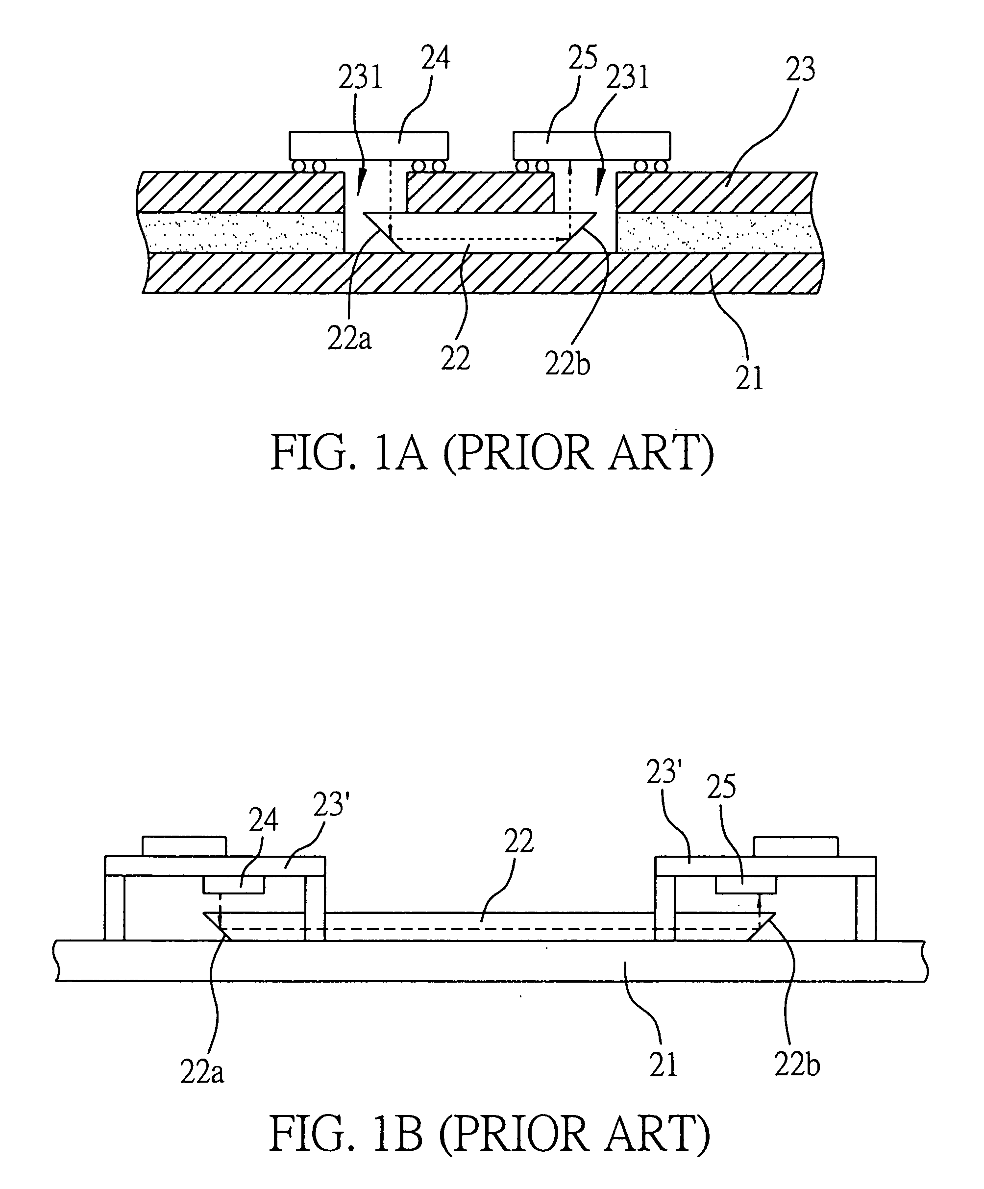
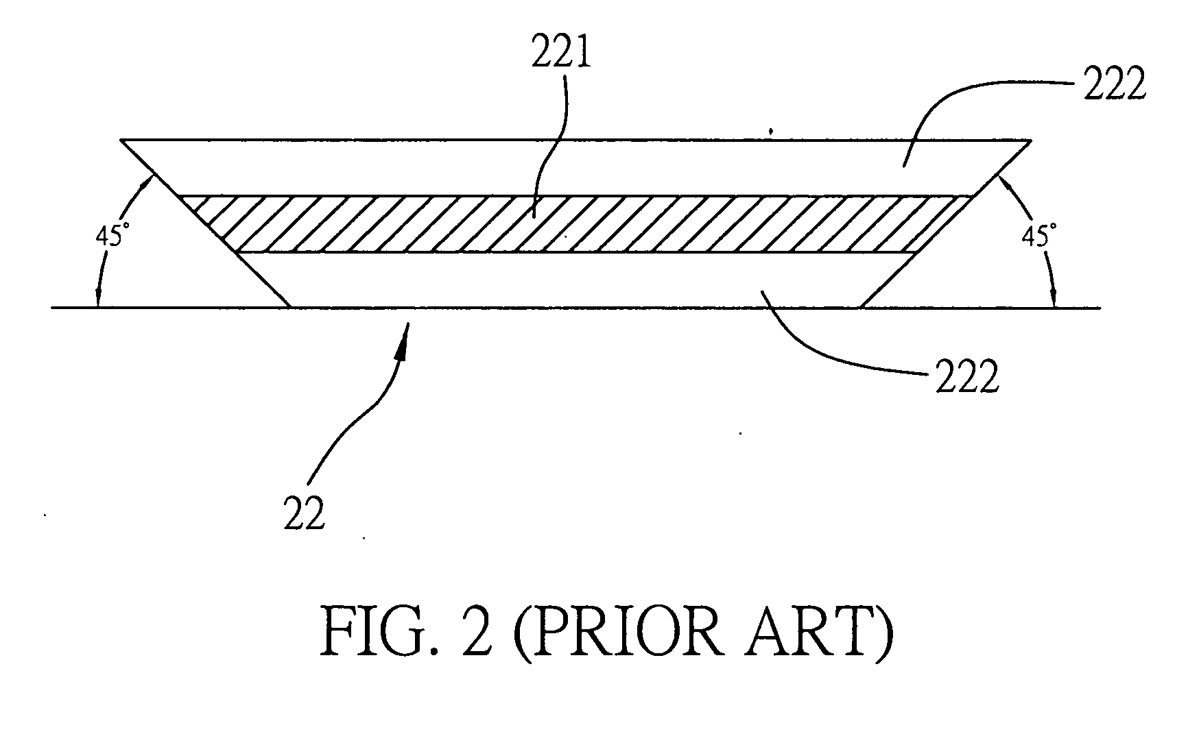
However, a drawback caused by the above conventional structure is that, it is difficult to form the pair of 45-degree reflection surfaces 22a, 22b at the two terminals of the waveguide 22.
The above conventional structure also requires high precision of
optical alignment and thus increases the fabrication costs thereof.
Further, since the photo beam must undergo two reflections via the reflection surfaces 22a, 22b, it may cause relatively greater loss of optical signals.
However, this arrangement increases the overall thickness of the structure by using the elevated circuit boards 23′ and similarly leads to the area occupying drawback, such that the requirement of having a compact size and a small profile cannot be satisfied for the structure.
Thus, the
assembly costs and difficulty in fabrication control of the structure are increased, thereby raising the fabrication costs.
Moreover, there is no heat dissipating structure provided for the optical
active component 24 and the optical receiving component 25, such that the overall heat dissipating effect is not satisfactory, and the optical
active component 24 and the optical receiving component 25 may easily be damaged by overheating.


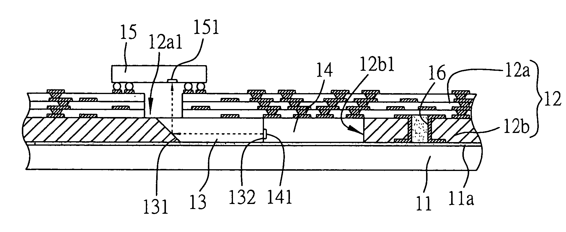