Control of signal line voltages on a bus

Inactive Publication Date: 2007-03-08
INFINEON TECH AG
View PDF4 Cites 4 Cited by
  • Summary
  • Abstract
  • Description
  • Claims
  • Application Information

AI Technical Summary

Benefits of technology

[0020] The apparatus is able to determine whether the voltage on the signal line is small, due to a heavy load on the signal line, or large, due to a lighter load on the signal line, by comparing the voltage on the signal line with the reference voltage. Then, the power

Problems solved by technology

However, not all the peripheral chips will require use of all the data and address lines on the bus.
So, some of the signal lines on the bus will be more heavily loaded than others and this will cause an unbalance in the loading between the pins.
This voltage dip is a problem that can cause bit error and system failure on a PCB board and the problem is, of course, exacerbated with higher temperature.
The voltage dip problem is one that may arise not just in S

Method used


Image

  • Control of signal line voltages on a bus
  • Control of signal line voltages on a bus
  • Control of signal line voltages on a bus

Examples


Embodiment Construction

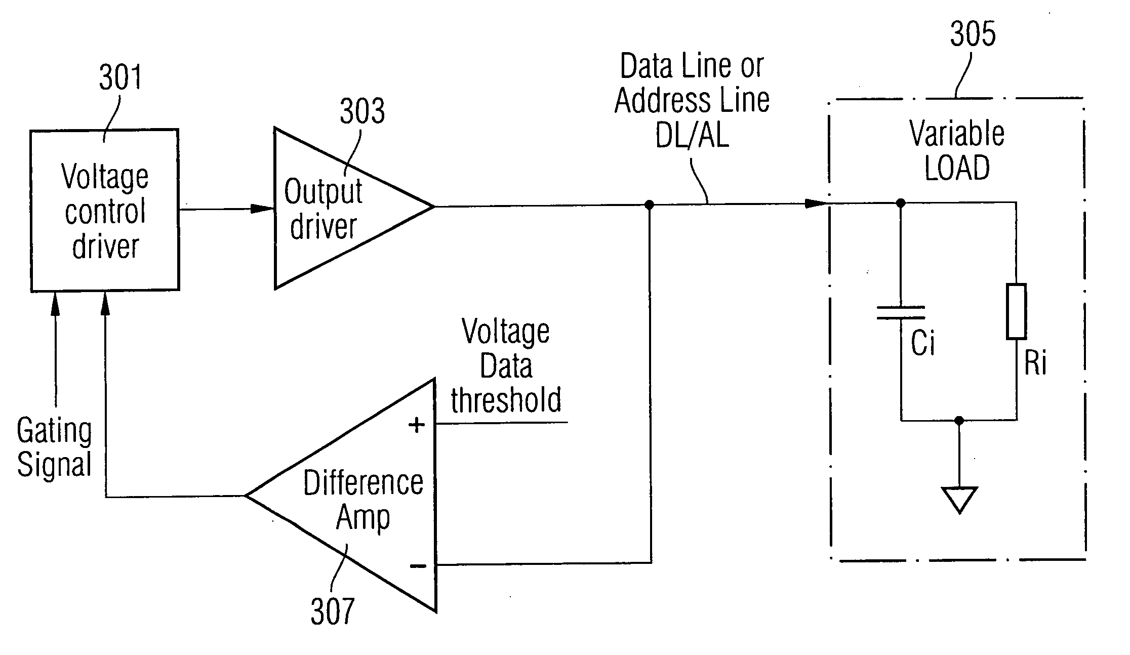
[0034] An exemplary embodiment of the invention will now be described with reference to FIG. 3 of the accompanying drawings, which is a diagram showing circuitry which can be used to monitor each data line and address line.

[0035] The circuitry includes a voltage control driver 301 connected to an output driver 303. The output driver 303 is connected to the particular data or address line to be monitored (termed DL / AL) and that data or address line is connected to a load 305. The load is a variable load since it depends on the number of peripheral chips sharing that data or address line. The voltage from the output driver 303 is compared with a threshold voltage in a differential amplifier 307. The output from the differential amplifier is input back into the voltage control driver 301. The voltage control driver 301 also receives a gating signal such as a write (WR) signal.

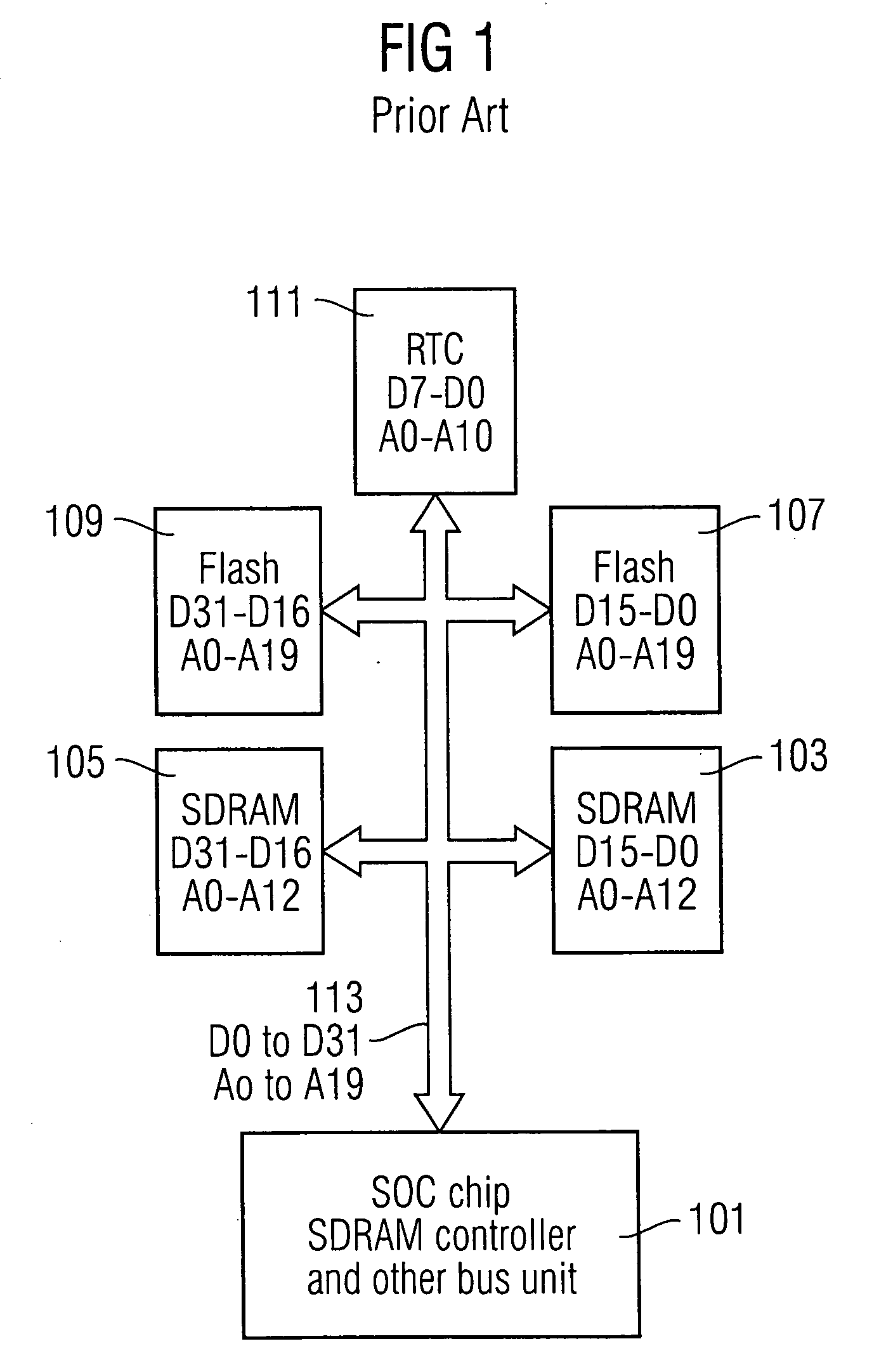
[0036] The circuitry can be used on each data and address line on the bus between an SoC (or other control ch...


PUM


Abstract

An apparatus is provided comprising a control chip, at least one peripheral chip connected to the control chip via a bus, the bus comprising a plurality of signal lines, and a control circuit coupled to each signal line of the bus. Each control circuit comprises a comparator for comparing voltage on the signal line with a reference voltage, and a driver connected to the comparator, for supplying power to the signal line, the driver being arranged to increase power supplied to the signal line if the voltage on the signal line is less than the reference voltage, the greater the difference between the voltage on the signal line and the reference voltage, the greater the increase in power supplied to the signal line, and to decrease power supplied to the signal line if the voltage on the signal line is greater than the reference voltage, the greater the difference between the voltage on the signal line and the reference voltage, the greater the decrease in power supplied to the signal line. There is also provided a method for monitoring each signal line of a bus connecting a control chip with at least one peripheral chip.

Description

TECHNICAL FIELD [0001] The invention relates to an apparatus and method for controlling power supplied to each signal line on a bus. In particular, the invention relates to an apparatus and method for controlling power supplied to each signal line on a bus, in which the bus connects a control chip to a plurality of peripheral chips and each peripheral chip requires a different number of the bus signal lines for operation. BACKGROUND [0002] Today, many communication products are System-on-Chip (SoC) products. SoC arrangements are ones in which the chip holds all the necessary hardware and electronic circuitry for a complete memory. In some arrangements, the SoC includes on-chip memory (RAM (Random Access Memory) and / or ROM (Read Only Memory)), a microprocessor, peripheral interfaces, I / O (input / output) logic control, data converters and other components required for the system. In other arrangements, the SoC has an embedded processor and an SDRAM (Synchronous Dynamic RAM) controller ...

Claims


Application Information

Patent Timeline
IPC IPC(8): G06F1/26
CPCG06F13/4077Y02B60/1235Y02B60/1228Y02D10/00
Inventor GOH, BAN HOK
Owner INFINEON TECH AG
Why Eureka
Try Eureka