

Method of manufacturing quad flat non-leaded semiconductor package
- Summary
- Abstract
- Description
- Claims
- Application Information
AI Technical Summary
Benefits of technology
Problems solved by technology
Method used
Image

Examples
first embodiment
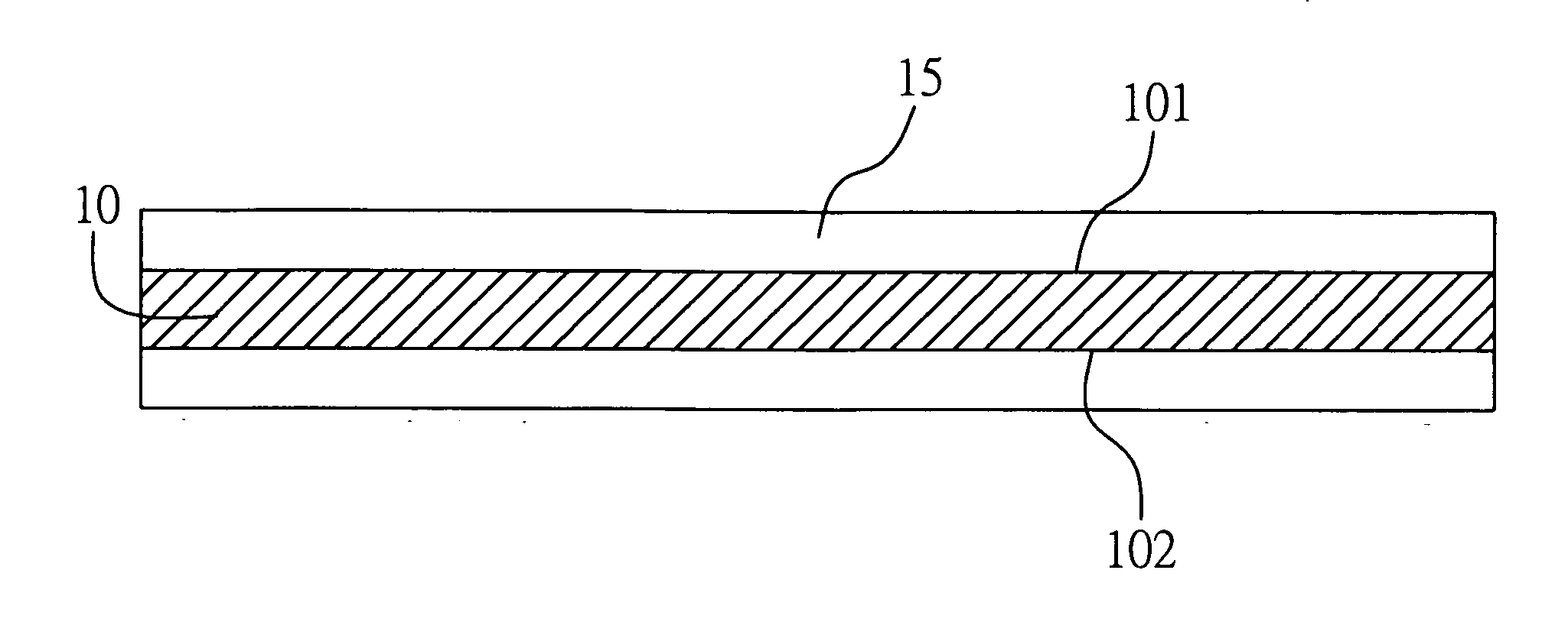
[0023]FIGS. 3A to 3I show steps of a method of manufacturing a quad flat non-leaded semiconductor package according to the present invention. As shown in FIG. 3A, a metal plate 10 made of such as copper is firstly prepared. The metal plate 10 has a first surface 101 and an opposed second surface 102. As the first surface 101 of the metal plate 10 serves as a die-bonding surface, it is defined with predetermined positions of a die pad 11 and a plurality of electrically conductive pads 12, wherein the positions of the electrically conductive pads 12 are located around the position of the die pad 11.
[0024] A resist layer 15 such as a dry film is formed on each of the first and second surfaces 101, 102 of the metal plate 10, and serves as a photoresist layer for use in subsequent exposure, development and etching processes. As shown in FIG. 3B, a plurality of openings 16 are formed in the resist layers 15 on the first and second surfaces 101, 102 of the metal plate 10 by the exposure, d...
fourth embodiment
[0030] Then, as shown in FIG. 6G, a molding process is performed such that the chip 30, the conductive bumps 50 and the first surface 101 of the metal plate 10 are encapsulated by an encapsulant 40. Moreover, as shown in FIG. 6H, an etching process is performed on the second surface 102 of the metal plate 10 so as to separate the electrically conductive pads 12 from each other. Finally, as shown in FIG. 6I, a singulation process is carried out to obtain the quad flat non-leaded semiconductor package according to the present invention.
[0031] Therefore, the method of the present invention allows the plating process of forming the metal plated layers and a lithography process to be completed on a panel-shaped metal plate, instead of a strip-shaped metal plate, before the molding process. That is, after defining the die pad and the electrically conductive pads, the fabrication processes such as die bonding, forming electrical connection and molding are performed, and then only a simple ...
PUM
 Abstract
Description
Claims
Application Information