Laser diode and laser diode device

a laser diode and laser diode technology, applied in the direction of lasers, semiconductor lasers, solid-state devices, etc., can solve the problem of difficult bonding of wires to the first electrode, and achieve the effect of convenient manufacturing and convenient mounting

Inactive Publication Date: 2007-03-22
SONY CORP
View PDF11 Cites 33 Cited by
  • Summary
  • Abstract
  • Description
  • Claims
  • Application Information

AI Technical Summary

Benefits of technology

[0009] In the laser diode according to the embodiment of the invention, an electrode of the plurality of electrodes except for at least one and the first conductive type layer are electrically connected to each other by the connecting portion, so the electrode (a first electrode) has the same potential as the first conductive type layer. Thereby, a region corresponding to the first electrode functions as a saturable absorption region, and a region corresponding to an electrode (a second electrode) of the plurality of electrodes except for the first electrode functions as a gain region, and the laser diode produces self-oscillation by an interaction between the regions. Moreover, the connecting portion is formed in the semiconductor layer, and self-oscillation can be produced without bonding a wire connected to a part having the same potential as the first conductive type layer to the first electrode. In other words, it is not necessary to arrange a wire on the first electrode.
[0010] In the laser diode according to the embodiment of the invention, a connecting portion is arranged in the semiconductor layer, and the first conductive type layer and the first electrode are electrically connected to each other by the connecting portion, so self-oscillation can be produced without separately arranging a wire on the first electrode. Thereby, as it is not necessary to arrange a wire on the first electrode, the laser diode can be easily mounted. Therefore, a laser diode device in which a heat radiation section, a device or the like is mounted on at least one of the plurality of electrodes side and the first conductive type layer side of the laser diode can be easily manufactured.

Problems solved by technology

Typically, an area of approximately 100 μm square is necessary to bond a wire; however, the first electrode typically does not have such a wide area, so it is very difficult to bond the wire to the first electrode.

Method used


Image

  • Laser diode and laser diode device
  • Laser diode and laser diode device
  • Laser diode and laser diode device

Examples


first embodiment

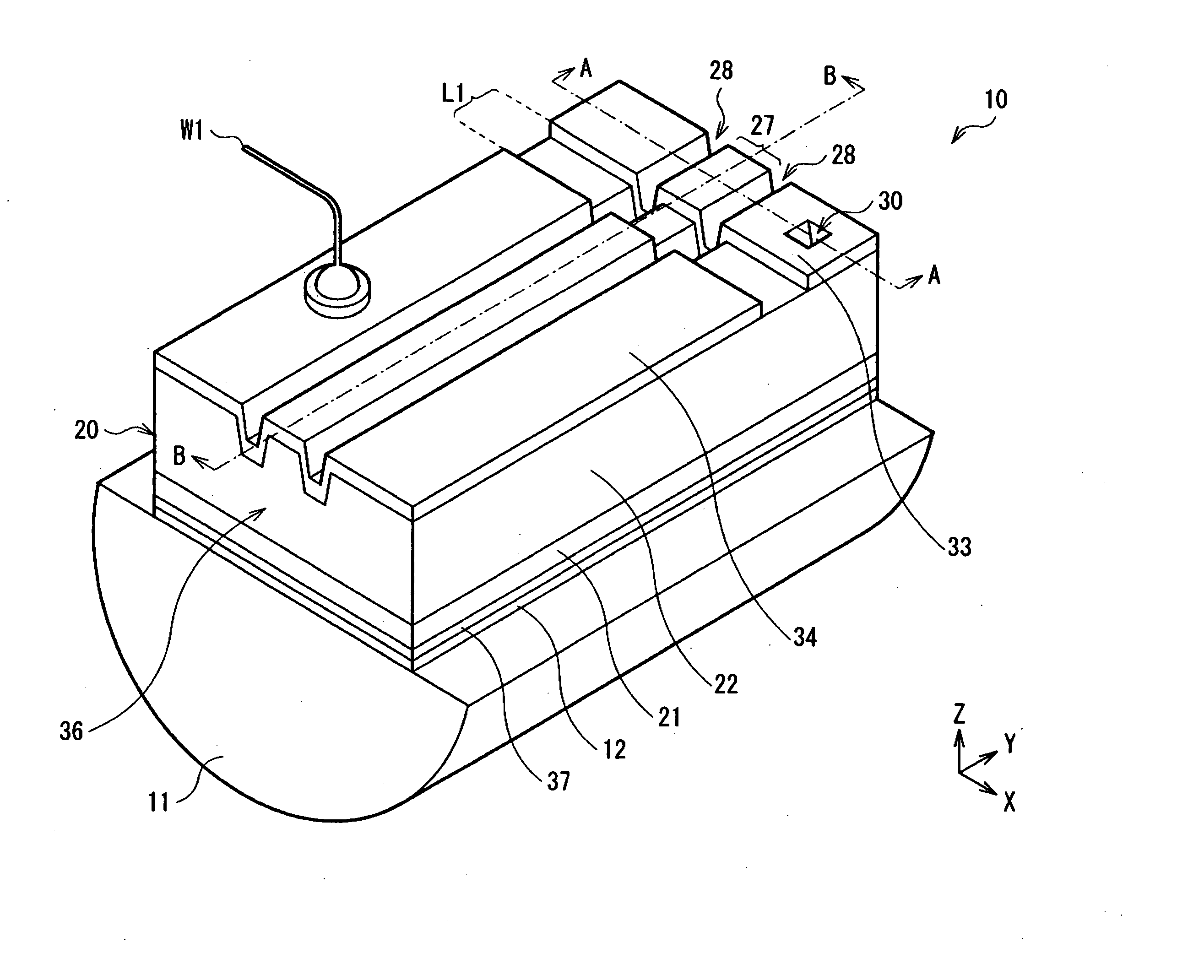
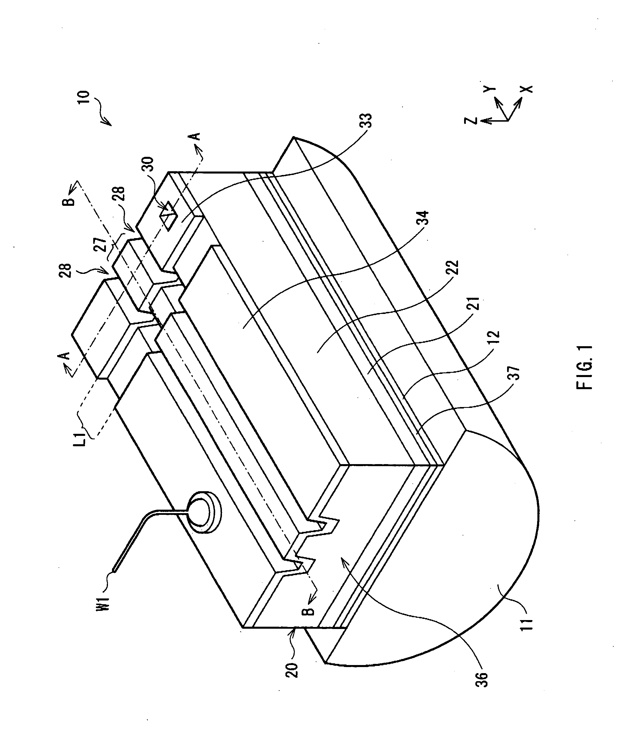
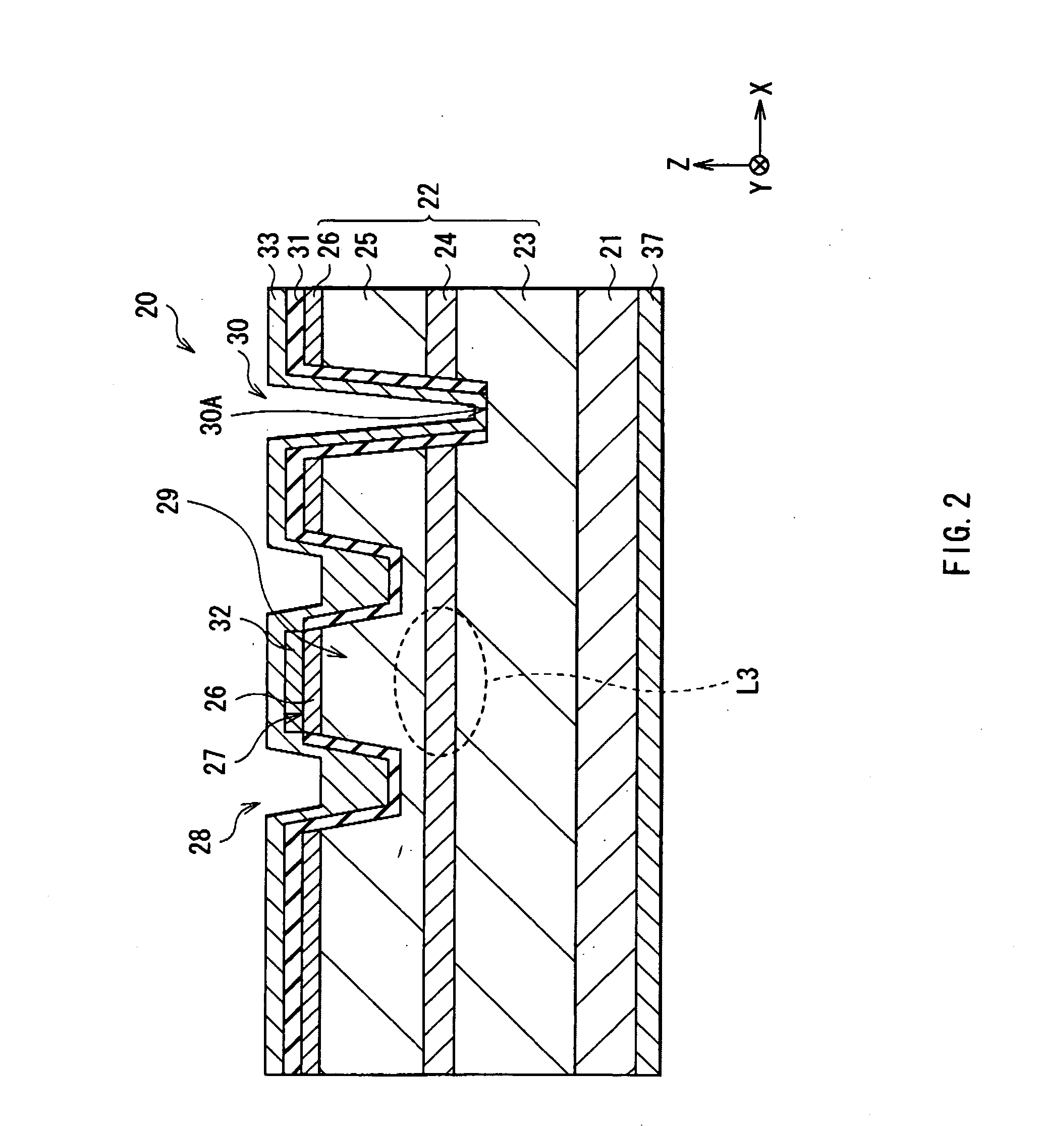
[0030]FIG. 1 is a perspective view of the structure of a laser diode device 10 according to a first embodiment of the invention. FIG. 2 is a sectional view taken along an arrow A-A of FIG. 1, and FIG. 3 is a sectional view taken along an arrow B-B of FIG. 1. FIGS. 1 through 3 are schematic views, so dimensions and shapes in FIGS. 1 through 3 are different from actual dimensions and shapes.

[0031] The laser diode device 10 is formed through mounting a laser diode 20 on a heat sink 11 (a heat radiation section) with a bonding layer 12 in between so as to face the p-side of the laser diode 20 up. The heat sink 11 is made of, for example, a material having electrical and thermal conductivity such as Cu (copper). The bonding layer 12 fixes the laser diode device 10 and the heat sink 11, and is made of, for example, a bonding material including AuSn or the like. Thereby, heat emitted from the laser diode 20 is dissipated via the heat sink 11, so the laser diode 20 is maintained at an appr...

second embodiment

[0069]FIG. 11 shows the structure of a laser diode device according to a second embodiment of the invention. FIG. 12 shows a sectional view taken along an arrow C-C of FIG. 11, and FIG. 13 shows a sectional view taken along an arrow D-D of FIG. 11. FIGS. 11 through 13 show schematic views, so dimensions and shapes in FIGS. 11 through 13 are different from actual dimensions and shapes.

[0070] The laser diode device is formed through mounting a laser diode 50 on the heat sink 11 (a heat radiation section) with the bonding layer 12 in between so as to face the p-side of the laser diode 50 up. The laser diode 50 is distinguished from the laser diode 20 including the saturable absorption region L3 in a part of a region corresponding to a predetermined region of the ridge 27 by the fact that a saturable absorption region L6 is included in a region corresponding to the groove 28. Therefore, the above difference will be mainly described in detail, and the same structures, functions and effe...

first modification

[First Modification]

[0086]FIG. 15 shows the structure of a laser diode device according to a first modification of the second embodiment. FIG. 15 is a schematic view, so dimensions and shapes in the FIG. 15 are different from actual dimensions and shapes. A laser diode 70 according to the modification is distinguished from the second embodiment by the fact that an ion implantation region L7 is included in a region corresponding to a region between the ridge 27 and the contact portion 53A in the active layer 24. The above difference will be mainly described in detail, and the same structures, functions and effects as those in the second embodiment will not be further described.

[0087] As described above, the ion implantation region L7 is formed in a region corresponding to a region between the ridge 27 and the contact portion 53A in the active layer 24. The ion implantation region L7 is formed through injecting ions including at least one kind selected from the group consisting of si...


PUM

PropertyMeasurementUnit
sizeaaaaaaaaaa
widthaaaaaaaaaa
lengthaaaaaaaaaa

Abstract

A laser diode capable of being easily mounted, and a laser diode device in which the laser diode is mounted are provided. A hole is disposed in a semiconductor layer, and a p-type electrode and an n-type semiconductor layer are electrically connected to each other by a bottom portion (a connecting portion) of the hole. Thereby, the p-type electrode has the same potential as the n-type semiconductor layer, and a saturable absorption region is formed in a region corresponding to a current path. Light generated in a gain region (not shown) is abosorbed in the saturable absorption region to be converted into a current. The current is discharged to a ground via the p-side electrode and the bottom portion, and an interaction between the saturable absorption region and the gain region is intitiated, thereby self-oscillation can be produced.

Description

CROSS REFERENCES TO RELATED APPLICATIONS [0001] The present invention contains subject matter related to Japanese Patent Application JP 2005-269904 filed in the Japanese Patent Office on Sep. 16, 2005, the entire contents of which being incorporated herein by reference. BACKGROUND OF THE INVENTION [0002] 1. Field of the Invention [0003] The present invention relates to a laser diode including two or more separated electrodes on a semiconductor layer and a laser diode device including the laser diode, and more specifically to a laser diode and a laser diode device capable of producing self-oscillation. [0004] 2. Description of the Related Art [0005] In recent years, as a low-noise laser diode (LD), a pulsation laser has been a focus of attention. The pulsation laser is a laser oscillating while generating self-excited vibration, and having low coherence and low optical feedback noise, so the pulsation laser is useful specifically for optical disks. For example, as described in Japane...

Claims


Application Information

Patent Timeline
Patent Type & Authority Applications(United States)
IPC IPC(8): H01S5/00
CPCB82Y20/00H01S5/0224H01S5/02272H01S5/02276H01S5/024H01S5/028H01L2224/48463H01S5/0425H01S5/22H01S5/2205H01S5/2214H01S5/34333H01S5/0422H01S5/04254H01S5/04256H01S5/04257H01S5/0234H01S5/02345H01S5/0237
Inventor KURAMOTO, MASARUASANO, TAKEHARU
Owner SONY CORP
Why Eureka
Try Eureka