Method of fabricating silicon nitride layer and method of fabricating semiconductor device

a silicon nitride and layer technology, applied in the direction of semiconductor devices, electrical devices, transistors, etc., can solve the problems of affecting the properties of metal silicide materials, uv curing treatment can barely meet the demands for higher tensile stress in most semiconductor fabrication processes, and the increase of tensile stress in the silicon nitride layer is quite limited

Active Publication Date: 2007-03-22
UNITED MICROELECTRONICS CORP
View PDF15 Cites 36 Cited by
  • Summary
  • Abstract
  • Description
  • Claims
  • Application Information

AI Technical Summary

Benefits of technology

[0010] Accordingly, at least one objective of the present invention is to provide a method of fabricating a silicon nitride layer that can effectively increase the tensile stress within the silicon nitride layer.
[0011] At least a second objective of the present invention is to provide a method of fabricating a semiconductor device that can effectively increase the driving current of the semiconductor device.
[0032] Since the ultraviolet curing treatment in the fabrication of silicon nitride layer provided in the present invention is carried out in a sub-atmospheric condition, overall tensile stress in the silicon nitride layer is increased.
[0033] Furthermore, since the semiconductor device fabricated according to the present invention can produce a silicon nitride layer with high tensile stress, the efficiency of electro-migration in the semiconductor device is improved and the driving current is increased.
[0034] In addition, the process window in an etching operation can be effectively increased when the silicon nitride layer is used as an etching stop layer.
[0035] On the other hand, obtaining a high tensile stress in the silicon nitride layer by performing an ultraviolet curing treatment at a lower surrounding temperature can avoid possible temperature-induced damage to the metal silicide layer.

Problems solved by technology

Thus, if a rapid thermal annealing process is applied to increase the stress in the silicon nitride etching stop layer, the high temperature created by the rapid thermal annealing operation will adversely affect the properties of the metal silicide material.
In addition, the UV curing treatment on a silicon nitride layer is carried out at normal atmospheric pressure so that the increase in tensile stress in the silicon nitride layer is quite limited.
Hence, the UV curing treatment can hardly meet the demands for higher tensile stress in most semiconductor fabrication processes.

Method used


Image

  • Method of fabricating silicon nitride layer and method of fabricating semiconductor device
  • Method of fabricating silicon nitride layer and method of fabricating semiconductor device
  • Method of fabricating silicon nitride layer and method of fabricating semiconductor device

Examples


Embodiment Construction

[0044] Reference will now be made in detail to the present preferred embodiments of the invention, examples of which are illustrated in the accompanying drawings. Wherever possible, the same reference numbers are used in the drawings and the description to refer to the same or like parts.

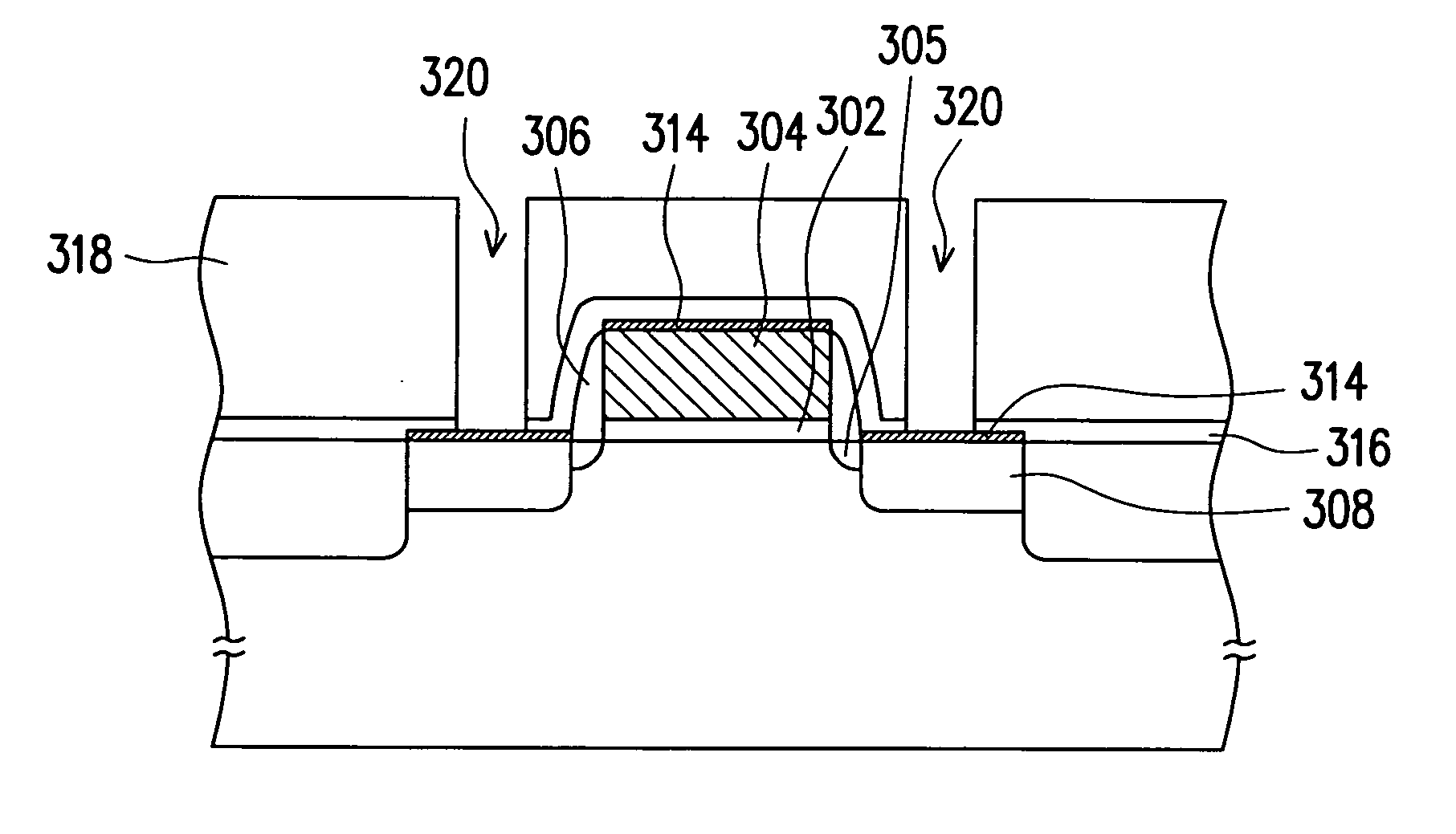
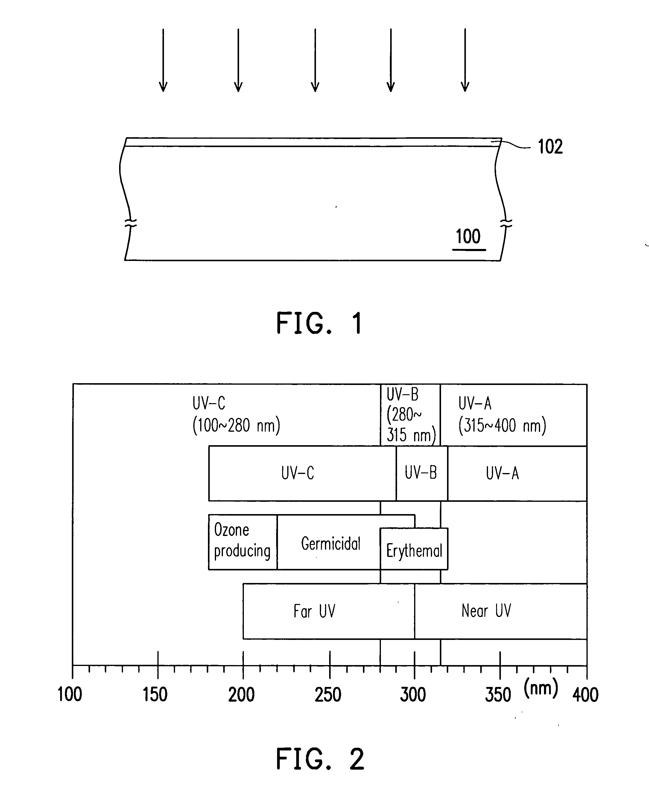
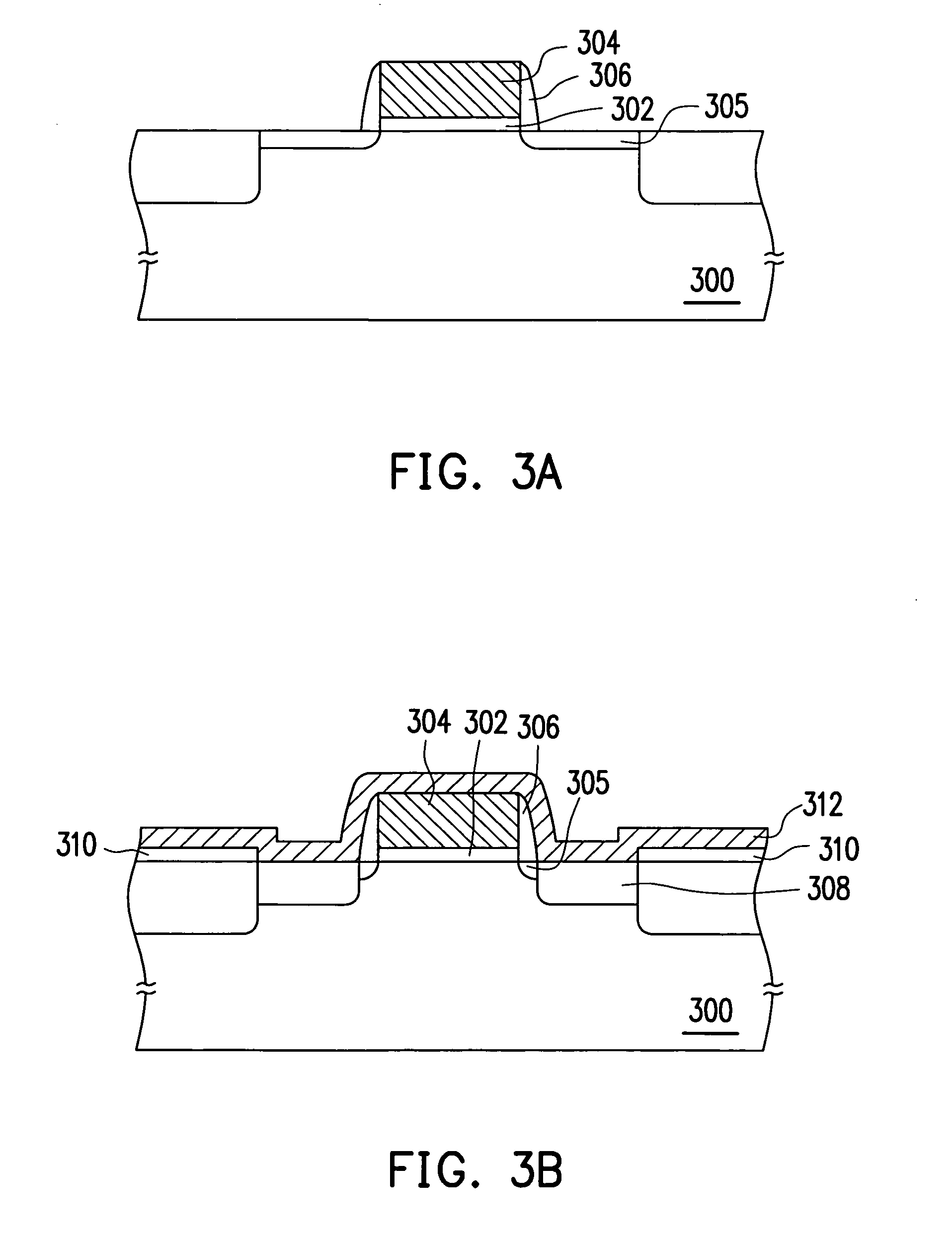
[0045]FIG. 1 is a schematic cross-sectional view of a silicon nitride layer according to one embodiment of the present invention. As shown in FIG. 1, the method of fabricating the silicon nitride layer in the present invention includes providing a substrate 100 such as a silicon substrate. Then, a silicon nitride layer 102 is formed on the substrate 100. The silicon nitride layer 102 is formed by performing a chemical vapor deposition process, for example, such as a plasma-enhanced chemical vapor deposition process, a low-pressure chemical vapor deposition process or an atomic layer chemical vapor deposition process.

[0046] Thereafter, an ultraviolet curing treatment of the silicon nitride layer 10...


PUM

PropertyMeasurementUnit
pressureaaaaaaaaaa
wavelengthaaaaaaaaaa
temperatureaaaaaaaaaa

Abstract

A method of fabricating a silicon nitride layer is described. First, a substrate is provided. Then, a silicon nitride layer is formed on the substrate. The silicon nitride layer is UV-cured in an atmosphere lower than the standard atmospheric pressure. Through the UV curing treatment, the tensile stress of the silicon nitride layer is increased.

Description

BACKGROUND OF THE INVENTION [0001] 1. Field of the Invention [0002] The present invention relates to a method of fabricating a silicon nitride layer. More particularly, the present invention relates to a method of fabricating a silicon nitride layer with a high tensile stress. [0003] 2. Description of the Related Art [0004] As semiconductor production shifted into the sub-micron regime, methods that can increase the driving current of NMOS and PMOS have become increasingly important especially for processes involving a feature size below 65 nm. Any increase in the driving current of NMOS and PMOS can significantly improve the time delay in the operating device. [0005] In recent years, many experts on semiconductor fabrication start to investigate the effects of a silicon nitride cap layer or silicon nitride etching stop layer with preloaded stress on the driving current of a device. Through such research, it has been found that a silicon nitride layer with tensile stress can increas...

Claims


Application Information

Patent Timeline
Patent Type & Authority Applications(United States)
IPC IPC(8): H01L21/336
CPCH01L29/665H01L29/7843H01L29/7833H01L29/6659
Inventor CHEN, NENG-KUOTSAI, TENG-CHUNLIAO, HSIU-LIEN
Owner UNITED MICROELECTRONICS CORP
Why Eureka
Try Eureka