Image sensor

a technology of image sensor and image, applied in the field of image sensor, can solve the problems of low signal to noise ratio, limited, and undesirable high yield, and achieve the effect of reducing fixed pattern nois

Inactive Publication Date: 2007-03-29
E2V TECH (UK) LTD
View PDF9 Cites 20 Cited by
  • Summary
  • Abstract
  • Description
  • Claims
  • Application Information

AI Technical Summary

Benefits of technology

[0026] Advantageously, a dark frame is integrated under same conditions as an image frame for processing the image frame to reduce fixed pattern noise caused by offset differences from separat...

Problems solved by technology

Such high yields may be undesirable, particularly for small pixels, e.g. of 40 μm or less, designed for the visible spectral region, where only one signal electron is generated per incident photon.
A common result when imaging energetic photons, is premature saturation of the pixel, and a low signal to noise ratio, limited by photon shot noise.
Even with a fixed thickness of a same scintillator material, obtaining a constant light level per unit x-ray dose to the sensor may not be straightforward in manufacture, for example, because of variations in density or porosity of the material.
However, matching of a scintillator to an imaging...

Method used


Image

  • Image sensor
  • Image sensor
  • Image sensor

Examples


Embodiment Construction

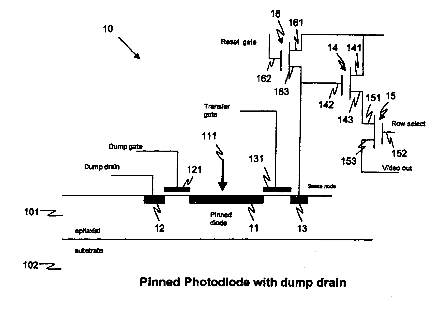
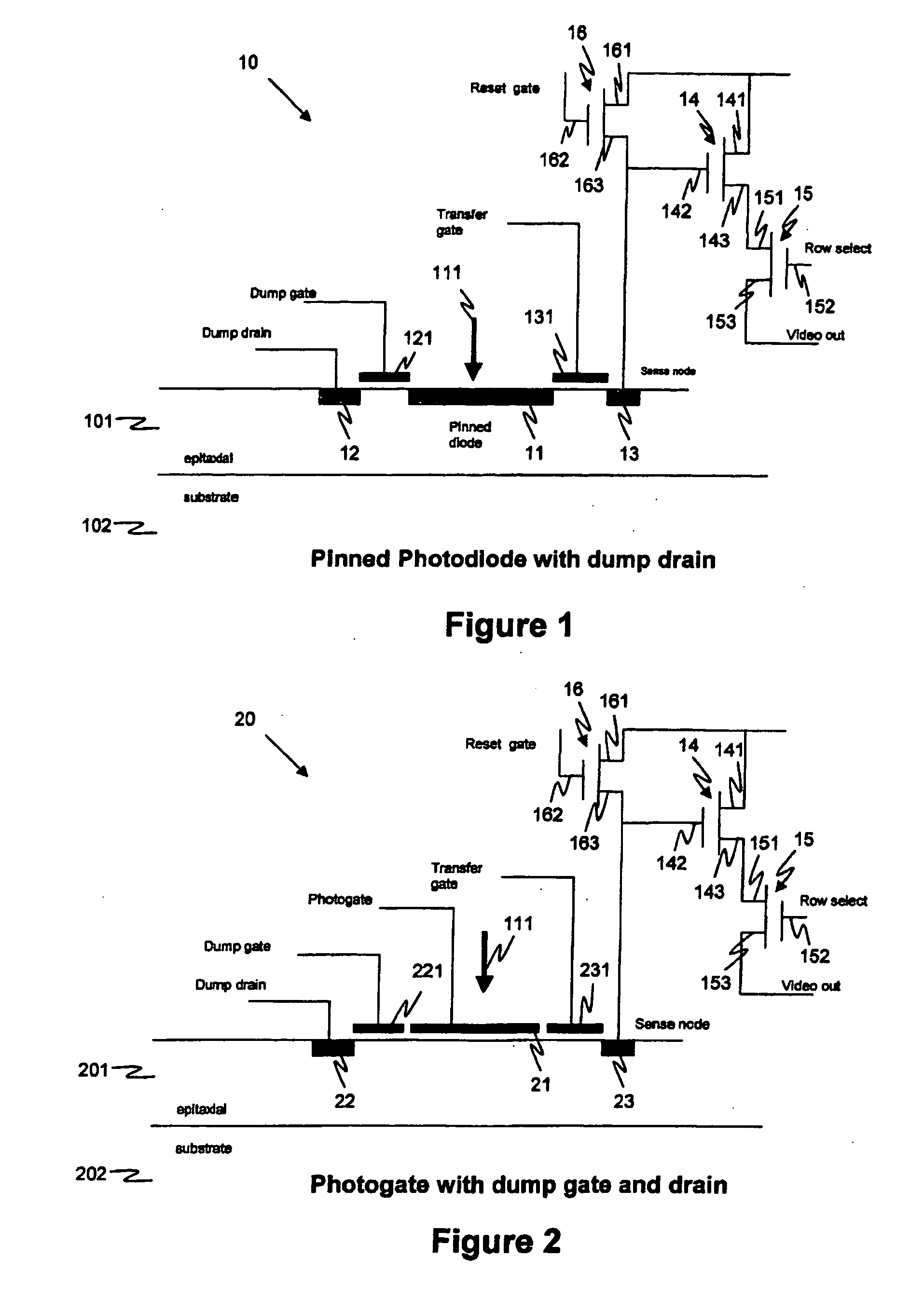
[0067] The invention may be applied to a scintillator-based image sensor in which structures in the pixel cause a charge dump / transfer action and so sub-divide the initial signal charge before it is accumulated in a storage or readout element of the pixel and subsequently converted to an output electrical signal.

[0068] Referring to FIG. 1, an x-ray sensor pixel 10 according to the invention includes a pinned photodiode 11, formed in an epitaxial layer 101 on a substrate 102, or built in silicon according to any known process, arranged to receive incident light 111 from a scintillator (not shown). Electrical charge generated by the incident light in the pinned diode 11 is transferable from the pinned diode to a dump drain 12 controlled by a dump gate 121. Charge is alternatively transferable to a sense node 13 controlled by a transfer gate 131. The sense node is connected in a known manner to a gate 142 of a buffer transistor 14. An output 143 of the buffer transistor is connected t...


PUM


Abstract

Effective sensitivity of a photodetector of an image sensor is controlled by partitioning signal charge from incident photons, thus producing a manageable yield and a consequently higher, photon shot noise limited, signal to noise ratio than in the prior art, when imaging high flux rates of energetic photons or particles, such as produced by x-ray generators. The invention may be applied, for example, to an image sensor with a photosensitive layer coupled to a charge collection/readout structure, e.g. photoconductor or scintillator on CMOS array, or to an intrinsically sensitive charge collection/readout structure, e.g. deep active layer CMOS. A radiation sensor pixel structure 10 for use in the invention includes a photodetector 11, a transfer gate 131 for controlling charge collection from the photodetector and a dump drain 12 controlled by a dump gate 121, arranged for selectively dumping charge to the dump drain means and collecting charge from the photodetector means, in a duty cycle 31, for varying effective sensitivity of the pixel structure. An image sensor containing such pixel structures may selectively be operated in an integration mode or a photon counting mode. Preferably the image sensor has imaging pixels and control circuitry arranged on a same semiconductor die, such as a CMOS semiconductor die.

Description

[0001] This invention relates to sensitivity control of an image sensor. In particular, the invention provides a method of partitioning a signal charge from incident photons, thus producing a manageable yield and a consequently higher, photon shot noise limited, signal to noise ratio than in the prior art, when imaging high flux rates of energetic photons or particles such as produced by x-ray generators. BACKGROUND OF THE INVENTION [0002] Image sensors which are used in a spectral range from hard UV, through x-rays to gamma-rays, i.e. with photon energies of 10 eV or greater, or in the imaging of energetic particles, e.g. free electrons, almost invariably produce a yield of many signal electrons per incident energetic photon or particle. Such high yields may be undesirable, particularly for small pixels, e.g. of 40 μm or less, designed for the visible spectral region, where only one signal electron is generated per incident photon. A common result when imaging energetic photons, is...

Claims


Application Information

Patent Timeline
IPC IPC(8): G01T1/24H01L27/146H04N5/235H04N5/359H04N5/365H04N5/3745
CPCH01L27/14609H01L27/14643H01L27/14663H01L27/14665H04N5/3745H04N5/2351H04N5/3592H04N5/365H04N5/23245H04N23/667H04N23/71H04N25/622H04N25/67H04N25/77
Inventor MOODY, IANBELL, RAYMOND THOMAS
Owner E2V TECH (UK) LTD
Why Eureka
Try Eureka