Method and apparatus for forming device features in an integrated electroless deposition system

a technology of electroless deposition and forming device, which is applied in the direction of superimposed coating process, resistive material coating, liquid/solution decomposition chemical coating, etc., can solve the problems of poor surface appearance of tantalum, tantalum nitride, titanium nitride, and high aspect ratio of nanometer-sized features

Inactive Publication Date: 2007-03-29
APPLIED MATERIALS INC
View PDF99 Cites 235 Cited by
  • Summary
  • Abstract
  • Description
  • Claims
  • Application Information

AI Technical Summary

Benefits of technology

[0012] Embodiments of the invention may further provide a method of processing a substrate in a substrate processing platform, comprising filing one or more recesses formed on a surface of the substrate with an electrolessly deposited metal layer, and inhibiting the growth of the electrolessly deposited metal layer generally above the top of the recesses formed in the surface of the substrate using a first electrode, a counter electrode and a power supply that is adapted to bias the first electrode relative to the counter electrode, wherein the first electrode is in electrical communication with at least a portion of the metal layer during at least a portion of the electroless deposition process.

Problems solved by technology

However, as the fringes of circuit technology are pressed, the shrinking dimensions of interconnects in VLSI and ULSI technology have placed additional demands on the processing capabilities.
Many traditional deposition processes have difficulty filling nanometer-sized structures where the aspect ratio exceeds 4:1, and particularly where the aspect ratio exceeds 10:1.
Therefore, there is a great amount of ongoing effort being directed at the formation of substantially void-free, nanometer-sized features having high aspect ratios.
Barrier layers comprising tantalum, tantalum nitride, titanium and titanium nitride are poor surfaces for nucleation of a subsequently electrolessly deposited material layer since native oxides of these barrier layer materials are easily formed.
However, if there are discontinuities in the seed layer across the surface, then a subsequently deposited layer may not form uniformly cover the seed layer.
The cost of ownership, which is affected by the cost of consumables used to keep each of these cluster tools running and the semiconductor fab space used to house all of these cluster tools, is very expensive for this process sequence, thus making it less competitive.
Also, one challenge is to fill very small features of varying depths and widths using this type of process sequence.
During typical PVD type device fabrication processes, the PVD deposited material will form regions that overhang the opening of the small features, which can hinder or prevent good gap fill of these features.
Further, the cost of consumables used to complete this process sequence, particularly during planarization processes, is high due to the amount of copper that needs to be removed during these steps.

Method used


Image

  • Method and apparatus for forming device features in an integrated electroless deposition system
  • Method and apparatus for forming device features in an integrated electroless deposition system
  • Method and apparatus for forming device features in an integrated electroless deposition system

Examples


Embodiment Construction

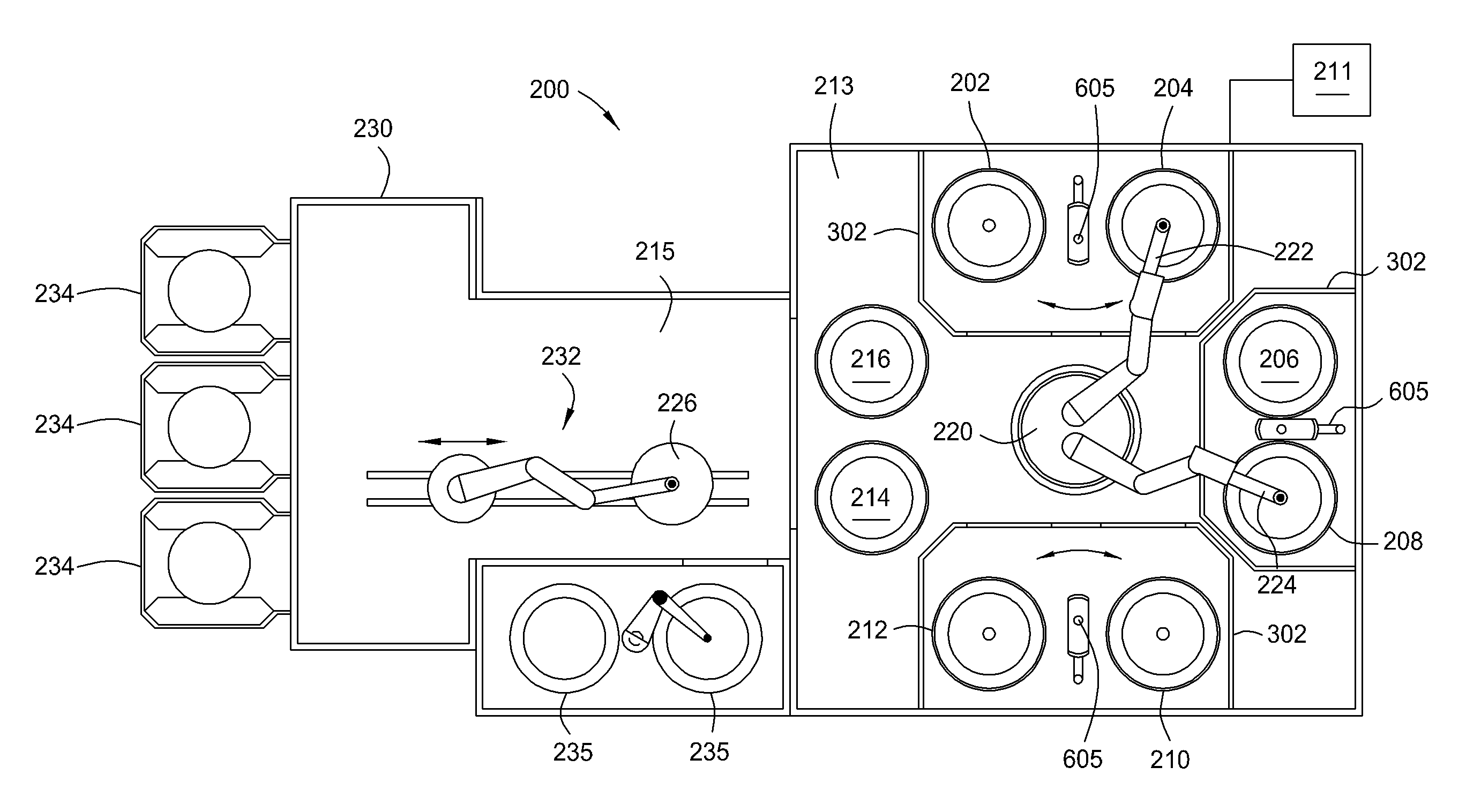
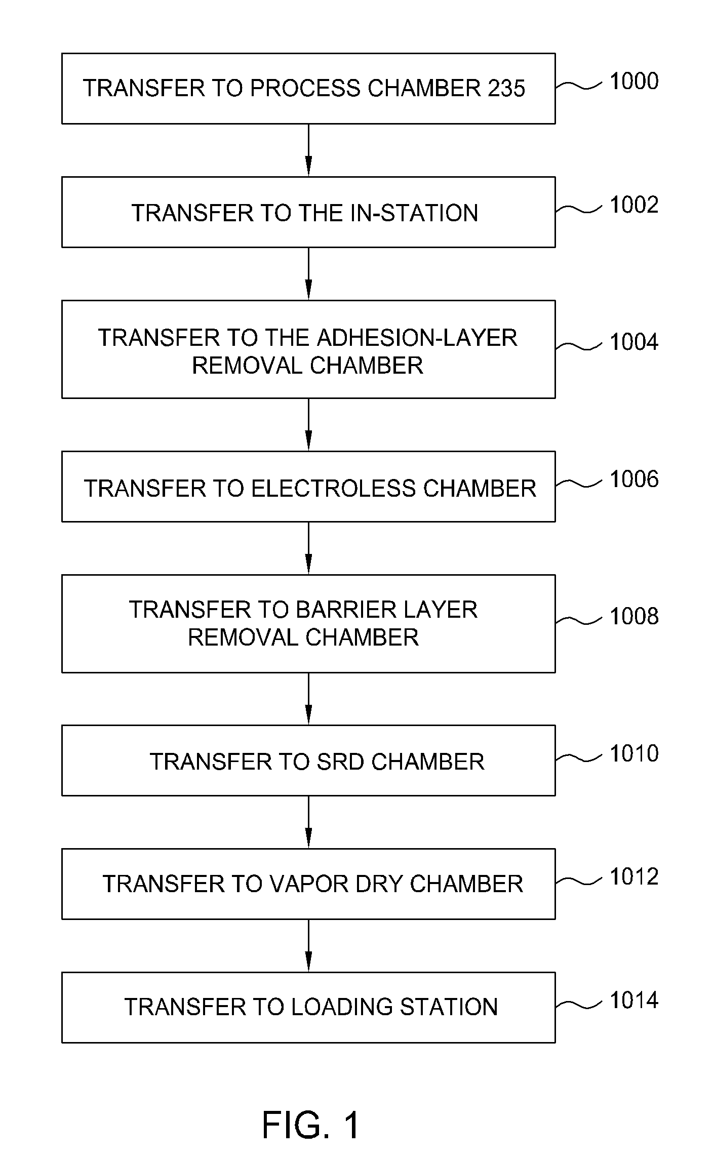
[0023] Embodiments of the invention generally provide a cluster tool that is configured to fill features formed on a substrate. An example of a typical substrate transferring sequence for a hybrid electroless / material removal platform is illustrated in FIG. 1, which is discussed below. More particularly, embodiments of the invention allow for the filling of interconnect or contact level features using one or more electroless fill process steps. A typical sequence for forming an interconnect includes depositing one or more non-conductive layers, etching at least one of the layer(s) to form one or more features therein, depositing a barrier layer in the feature(s) and depositing one or more conductive layers, such as copper, to fill the feature.

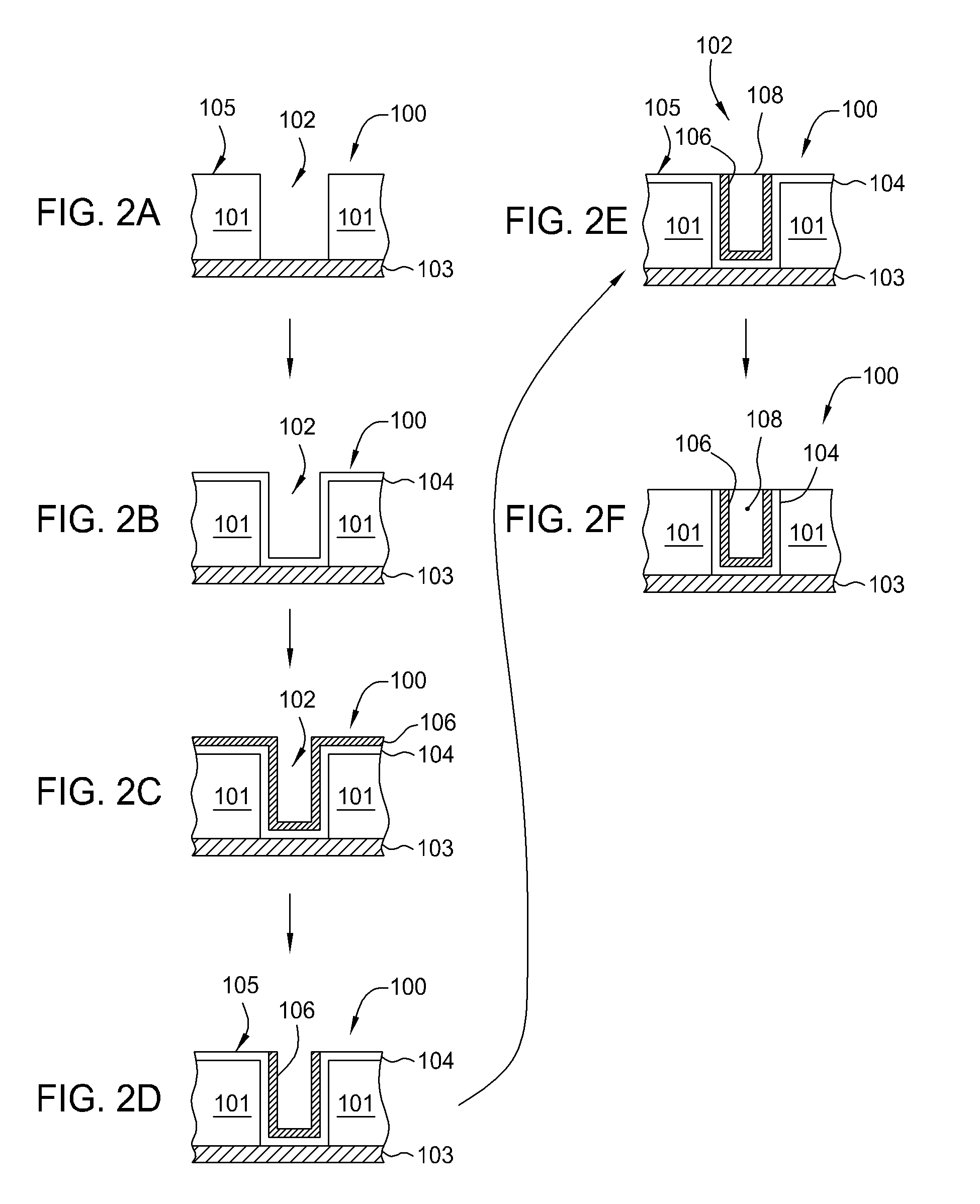
[0024]FIGS. 2A-2F illustrate a cross-sectional view of a feature 102 as the various processing steps of a process sequence 110 (FIG. 3) are performed on a substrate 100. FIG. 2A illustrates a cross-sectional view of substrate 100 having a fiel...


PUM

PropertyMeasurementUnit
thickaaaaaaaaaa
thicknessaaaaaaaaaa
adhesionaaaaaaaaaa

Abstract

Embodiments of the invention generally provide a cluster tool that is configured to electrolessly fill features formed on a substrate. More particularly, embodiments of the invention are used to integrate the filling of an interconnect or contact level feature using an electroless fill process and material removal steps. A typical sequence for forming an interconnect includes depositing one or more non-conductive layers, etching at least one of the layer(s) to form one or more features therein, depositing a barrier layer in the feature(s) and depositing one or more conductive layers, such as copper, to fill the feature.

Description

CROSS-REFERENCE TO RELATED APPLICATIONS [0001] This application claims benefit of U.S. Provisional Patent Application Ser. No. 60 / 719,440, filed Sep. 21, 2005, which is herein incorporated by reference.BACKGROUND OF THE INVENTION [0002] 1. Field of the Invention [0003] Embodiments of the invention generally relate to a method and apparatus for depositing materials within a feature using an integrated electroless deposition system. [0004] 2. Description of the Related Art [0005] Reliably producing nanometer-sized features is one of the key technologies for the next generation of very large scale integration (VLSI) and ultra large scale integration (ULSI) of semiconductor devices. However, as the fringes of circuit technology are pressed, the shrinking dimensions of interconnects in VLSI and ULSI technology have placed additional demands on the processing capabilities. Contact metallization and multilevel interconnect metallization lie at the heart of this technology require precise p...

Claims


Application Information

Patent Timeline
Patent Type & Authority Applications(United States)
IPC IPC(8): H05K3/00B05D3/00B05D1/18C23F1/00
CPCC23C18/1608C23C18/1619C23F3/00C23F3/04H01L21/02074H01L21/02087H05K2201/09563H01L21/6723H01L21/76846H01L21/76849H01L21/76879H05K3/045H05K3/422H01L21/288
Inventor SHANMUGASUNDRAM, ARULKUMARWEIDMAN, TIMOTHY
Owner APPLIED MATERIALS INC
Why Eureka
Try Eureka