Hardware acceleration system for logic simulation using shift register as local cache with path for bypassing shift register

a logic simulation and shift register technology, applied in the field of shift register as local cache with bypass path, can solve the problems of high processing speed and a large number of operations, hardware emulators typically require high cost, and software simulators typically are very slow, so as to simplify the hardware design of the simulation processor and reduce the instruction length

Inactive Publication Date: 2007-03-29
LIGA SYST
View PDF37 Cites 28 Cited by
  • Summary
  • Abstract
  • Description
  • Claims
  • Application Information

AI Technical Summary

Benefits of technology

[0011] The present invention provides a simulation processor for performing logic simulation of logic operations, where intermediate values generated by the simulation processor during the logic simulation are stored in shift registers. The simulation processor includes a plurality of processor units and an interconnect system (e.g., a crossbar) that communicatively couples the processor units to each other. As compared to an addressable register, the use of a shift register as local cache reduces the instruction length and also simplifies the hardware design of the simulation processor.

Problems solved by technology

Simulation of a logic design typically requires high processing speed and a large number of operations due to the large number of gates and operations and the high speed of operation typically present in the logic design for modern semiconductor chips.
Unfortunately, software simulators typically are very slow.
Unfortunately, hardware emulators typically require high cost because the number of hardware circuits in the emulator increases according to the size of the simulated logic design.
In addition, hardware-accelerated simulators typically are faster than software simulators due to the hardware acceleration produced by the simulation processor.
However, hardware-accelerated simulators generally require that instructions be loaded onto the simulation processor for execution and the data path for loading these instructions can be a performance bottleneck.
This input address signal typically is included as part of the instruction sent to the processor element, which can significantly increase the instruction length and exacerbate the instruction bandwidth bottleneck.
This adds to the cost, size and complexity of the simulation processor.

Method used


Image

  • Hardware acceleration system for logic simulation using shift register as local cache with path for bypassing shift register
  • Hardware acceleration system for logic simulation using shift register as local cache with path for bypassing shift register
  • Hardware acceleration system for logic simulation using shift register as local cache with path for bypassing shift register

Examples


first embodiment

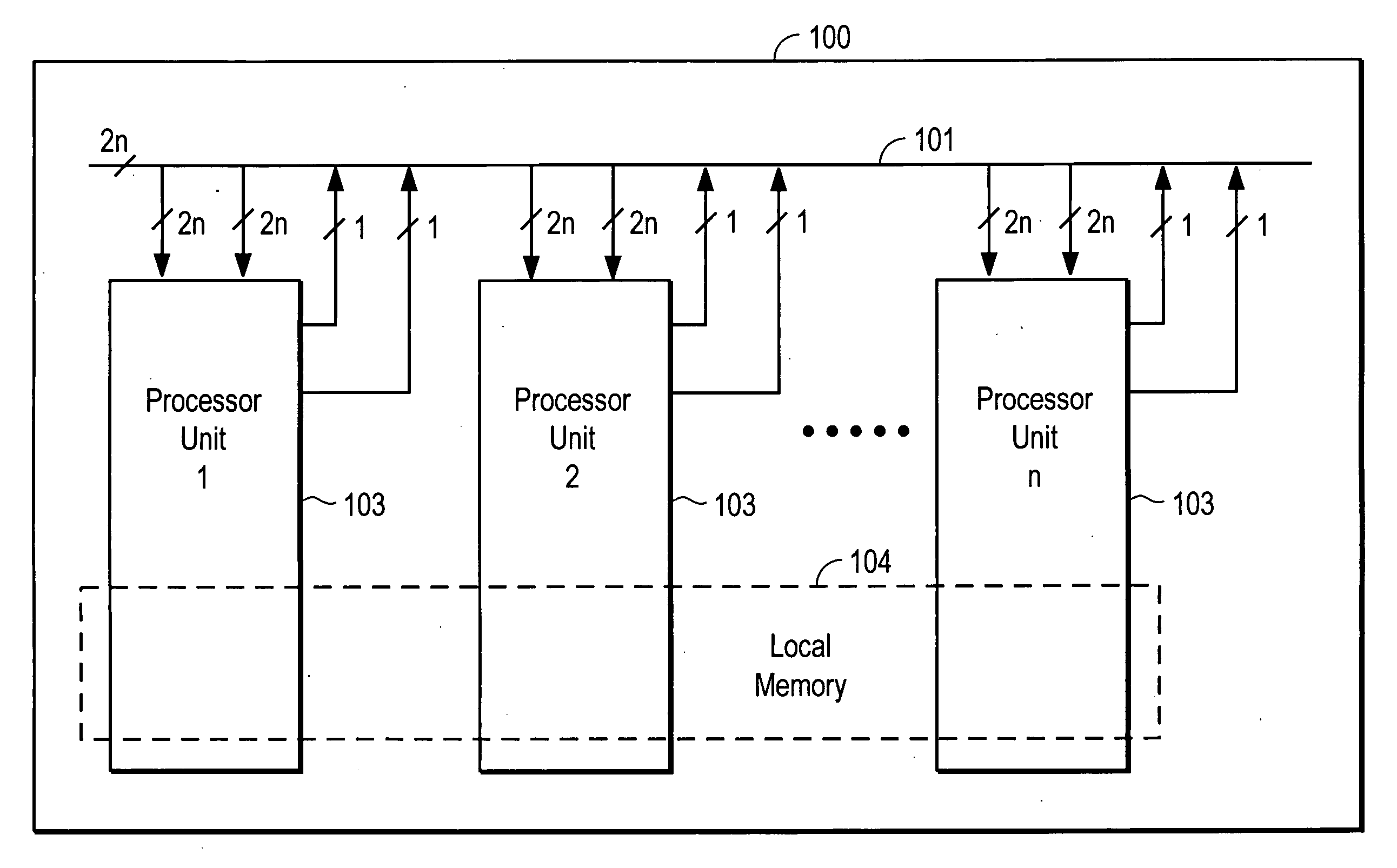
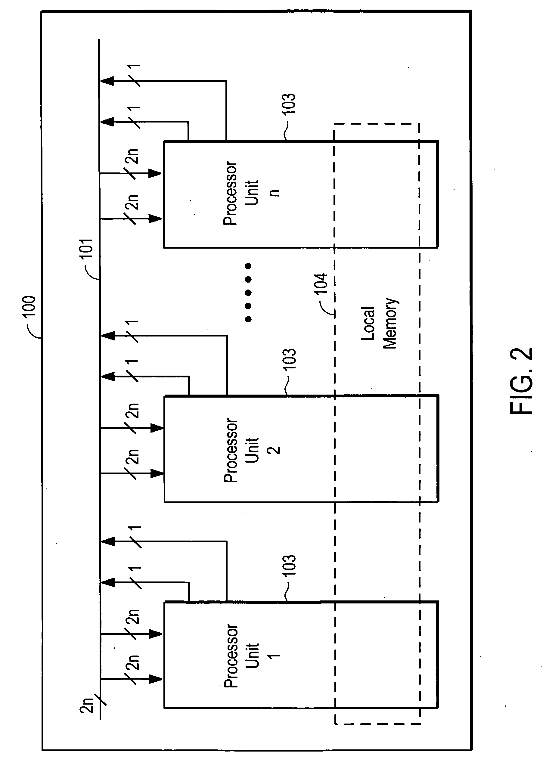
[0054]FIG. 3 is a circuit diagram illustrating a single processor unit 103 of the simulation processor 100 in the hardware accelerated logic simulation system according to the present invention. Each processor unit 103 includes a processor element (PE) 302, a shift register 308, an optional memory 326, multiplexers 304, 306, 310, 312, 314, 316, 320, 324, and flip flops 318, 322. The processor unit 103 is controlled by instructions 118 (shown as 382 in FIG. 3). The instruction 382 has fields P0, P1, Boolean Func, EN, XB0, XB1, and Xtra Mem in this example. Let each field X have a length of X bits. The instruction length is then the sum of P0, P1, Boolean Func, EN, XB0, XB1, and Xtra Mem in this example.

[0055] A crossbar 101 interconnects the processor units 103. The crossbar 101 has 2n bus lines, if the number of PEs 302 or processor units 103 in the simulation processor 100 is n and each processor unit has two inputs and two outputs to the crossbar. In a 2-state implementation, n re...

second embodiment

[0081]FIG. 4 illustrates a single processor unit 103 of the simulation processor in the hardware accelerated logic simulation system according to the present invention. Each processor unit 103 includes a processor element (PE) 302, a shift register 308, a memory 326, multiplexers 304, 306, 310, 312′, 314′, 316, 320, 324, 386 and flip flops 318, 322. The processor unit 103 is controlled by instructions 383, which have fields P0, P1, Boolean Func, EN, XB0′, XB1′ (XB1′=XB0′+1), and Xtra Mem (optional). A crossbar 101 interconnects each of the processor units 103. The crossbar 101 has 2n bus lines, if the number of PEs 302 or processor units 103 in the simulation processor 100 is n and each processor unit has two inputs and two outputs to the crossbar.

[0082] The processor unit shown in FIG. 4 is the same as the one shown in FIG. 3, with one significant difference. In FIG. 3, multiplexer 312 could select any of they entries in shift register 308, as could multiplexer 314. In FIG. 4, whil...

third embodiment

[0090]FIG. 5 is a circuit diagram illustrating a single processor unit of the simulation processor according to the present invention. The processor unit shown in FIG. 5 is the same as the one shown in FIG. 3, with a few significant differences. As compared to the processor unit in FIG. 3, the processor unit of FIG. 5 additionally includes multiplexers 506, 514, 508, and the EN signal of the instruction word 530 has three bits (en0, en1, en2) for defining the operation modes. An additional enable signal enA is included and is derived from en0 and en2 using the following formula: enA=en0*en2+˜en0*˜en2. Also note that the memory 326 is addressed by the address 532 comprised of only XB0 and XB1, without the Xtra Mem bit, for simplicity in the drawings. Also, in FIGS. 5, 5A through 5F, the relevant multiplexers are shown such that if the corresponding control bit value is 0, the uppermost or leftmost input is selected, and if the corresponding control bit value is 1, the lowermost or ri...


PUM


Abstract

A simulation processor includes multiple processor units and an interconnect system that communicatively couples the processor units to each other. Each of the processor units includes a processor element configurable to simulate at least a logic operation, and a shift register for storing intermediate values generating during the logic simulation. Each of the processor units further includes one or more multiplexers for selecting one of the entries of the shift register as outputs to be coupled to the interconnect system. Each of the processor units can also include one or more bypass multiplexers coupled between the output of the processor element and the interconnect system, for providing a path for bypassing the shift register to provide the output of the processor element directly to the interconnect system.

Description

CROSS-REFERENCE TO RELATED APPLICATION [0001] This application is a continuation-in-part application of, and claims priority under 35 U.S.C. §120 from, co-pending U.S. patent application Ser. No. 11 / 238,505, entitled “Hardware Acceleration System for Logic Simulation Using Shift Register as Local Cache,” filed on Sep. 28, 2005.BACKGROUND OF THE INVENTION [0002] 1. Field of the Invention [0003] The present invention relates generally to VLIW (Very Long Instruction Word) processors, including for example simulation processors that may be used in hardware acceleration systems for logic simulation. More specifically, the present invention relates to the use of shift registers as the local cache in such processors. [0004] 2. Description of the Related Art [0005] Simulation of a logic design typically requires high processing speed and a large number of operations due to the large number of gates and operations and the high speed of operation typically present in the logic design for mode...

Claims


Application Information

Patent Timeline
Patent Type & Authority Applications(United States)
IPC IPC(8): G06F15/00
CPCG06F17/5022G06F30/33
Inventor VERHEYEN, HENRY T.WATT, WILLIAM
Owner LIGA SYST
Why Eureka
Try Eureka