Hardware acceleration system for logic simulation using shift register as local cache
Inactive Publication Date: 2007-03-29
LIGA SYST
View PDF32 Cites 31 Cited by
Summary
Abstract
Description
Claims
Application Information
AI Technical Summary
This helps you quickly interpret patents by identifying the three key elements:
Problems solved by technology
Method used
Benefits of technology
Benefits of technology
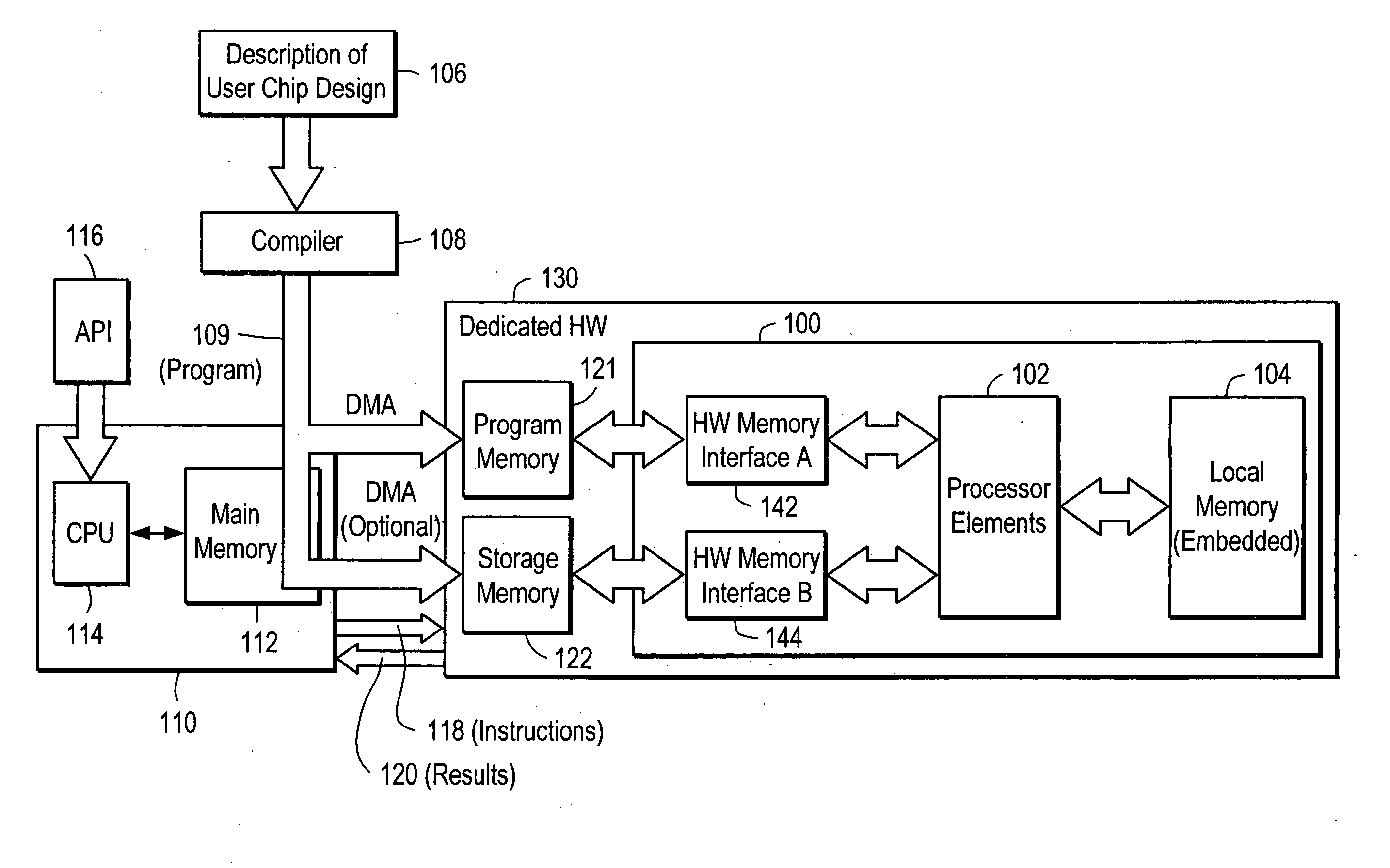
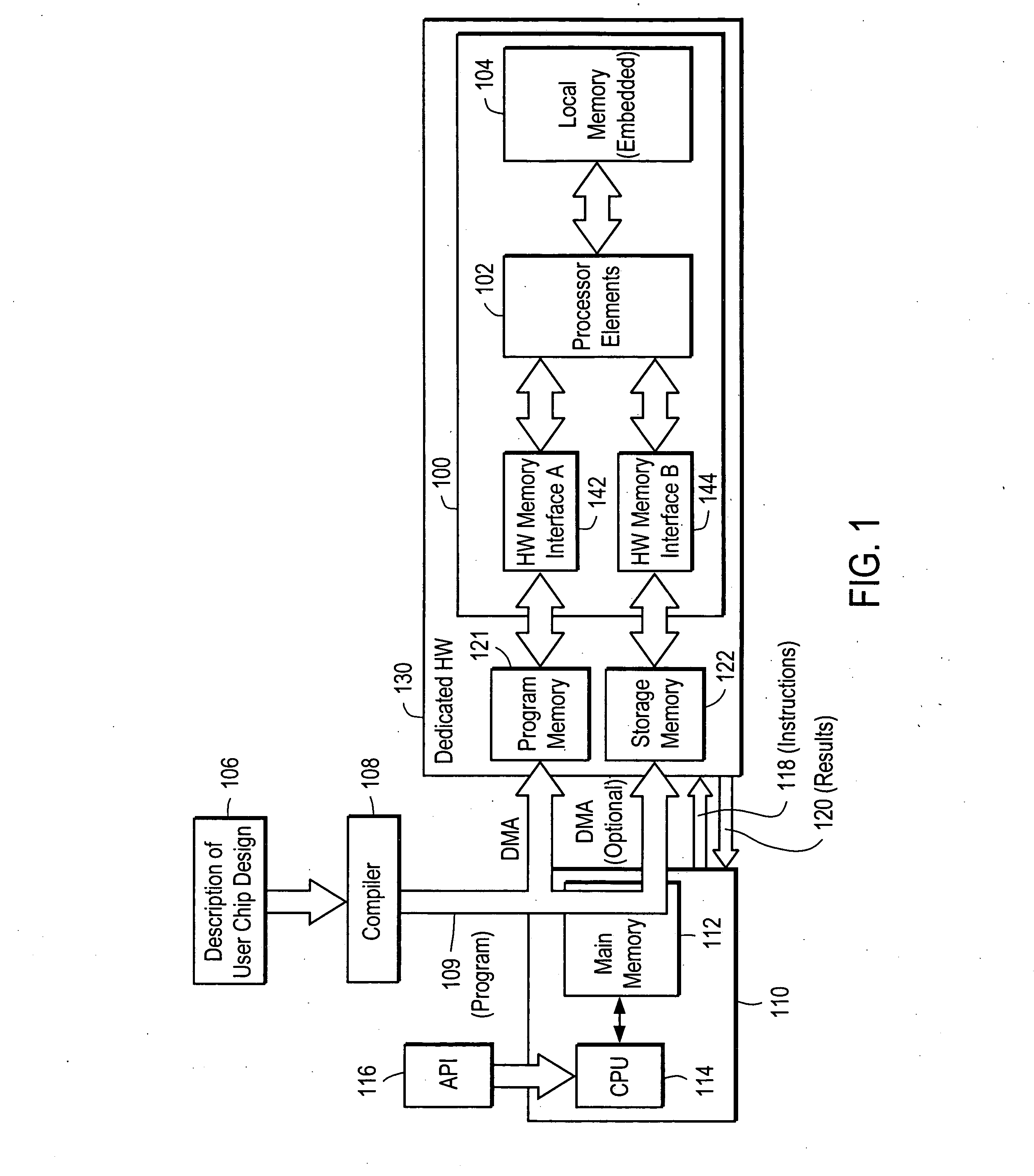
[0009] The present invention provides a simulation processor for performing logic simulation of logic gates, where intermediate values generated by the simulation processor during the logic simulation are stored in shift registers. The simulation process includes a plurality of processor units and an interconnect system (e.g., a crossbar) that communicatively couples the processor units to each other. As compared to an addressable register, the use of a shift register as local cache reduces the instruction length and also simplifies the hardware design of the simulation processor.
[0013] The simulation processor of the present invention has the advantage that it may reduce the instruction length, because the shift register does not require any input address signals. Also, input multiplexers are not necessarily required to select cells of the shift register. The simulation process of the present invention has the additional advantage that the shift register is interconnected with the local memory in such a way that a store mode and a load mode for the processor element are non-blocking with respect to an evaluation mode. That is, the store mode and the load mode may be performed simultaneously with the evaluation mode.
Problems solved by technology
Simulation of a logic design typically requires high processing speed and a large number of operations due to the large number of gates and operations and the high speed of operation typically present in the logic design for modern semiconductor chips.
Unfortunately, software simulators typically are very slow.
Unfortunately, hardware emulators typically require high cost because the number of hardware circuits in the emulator increases according to the size of the simulated logic design.
In addition, hardware-accelerated simulators typically are faster than software simulators due to the hardware acceleration produced by the simulation processor.
However, hardware-accelerated simulators generally require that instructions be loaded onto the simulation processor for execution and the data path for loading these instructions can be a performance bottleneck.
This input address signal typically is included as part of the instruction sent to the processor element, which can significantly increase the instruction length and exacerbate the instruction bandwidth bottleneck.
This adds to the cost, size and complexity of the simulation processor.
Method used
Image
Click on the blue label to locate the original text in one second.
Reading with bidirectional positioning of images and text.
Examples
first embodiment
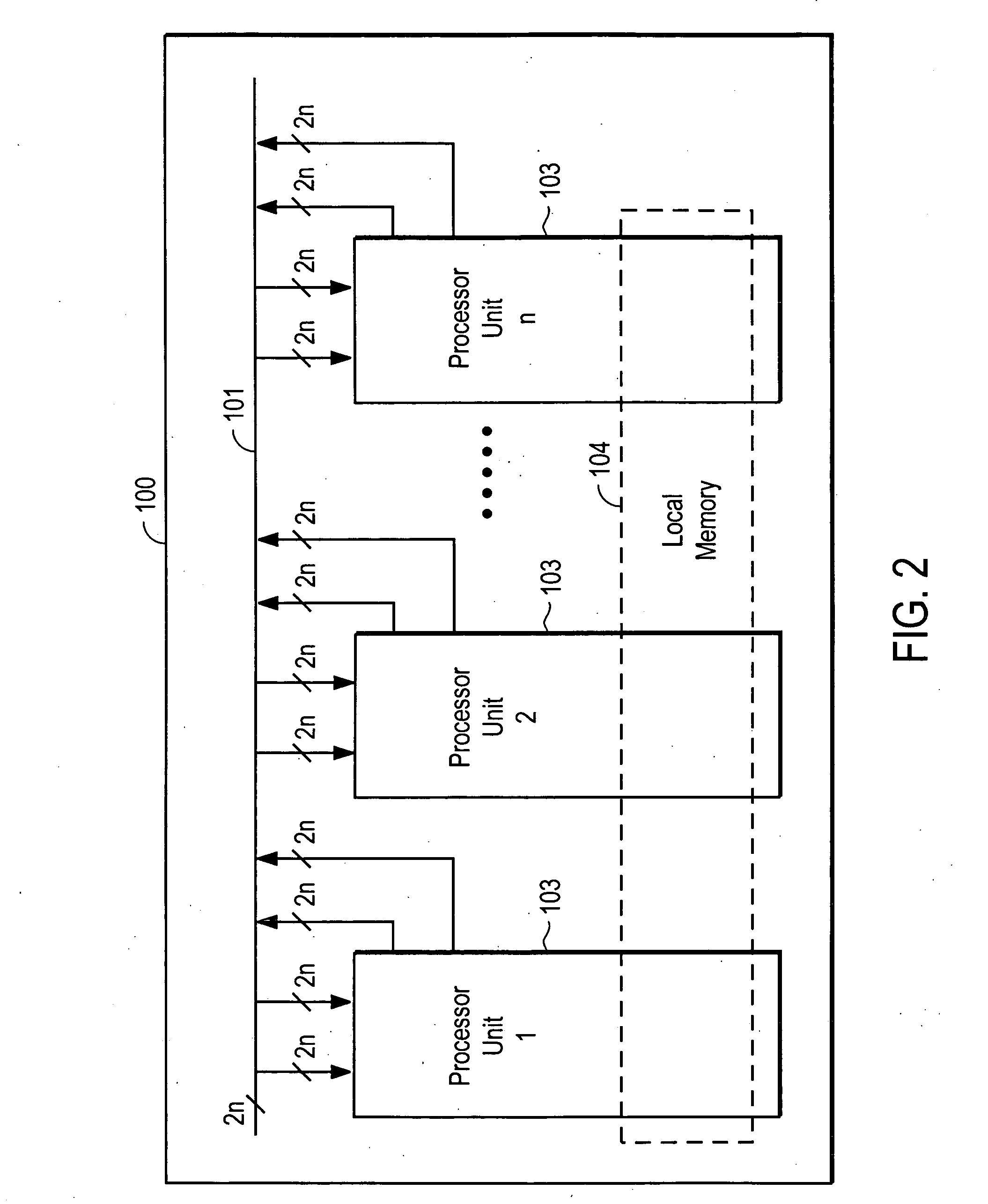
[0031]FIG. 3 is a circuit diagram illustrating a single processor unit 103 of the simulation processor 100 in the hardware accelerated logic simulation system according to the present invention. Each processor unit 103 includes a processor element (PE) 302, a shift register 308, an optional memory 326, multiplexers 304, 306, 310, 312, 314, 316, 320, 324, and flip flops 318, 322. The processor unit 103 is controlled by instructions 118 (shown as 382 in FIG. 3). The instruction 382 has fields P0, P1, Boolean Func, EN, XB0, XB1, and Xtra Mem in this example. Let each field X have a length of X bits. The instruction length is then the sum of P0, P1, Boolean Func, EN, XB0, XB1, and Xtra Mem in this example. A crossbar 101 interconnects the processor units 103. The crossbar 101 has 2n bus lines, if the number of PEs 302 or processor units 103 in the simulation processor 100 is n and each processor unit has two inputs and two outputs to the crossbar. In a 2-state implementation, n represen...
second embodiment
[0052]FIG. 4 is a circuit diagram illustrating a single processor unit 103 of the simulation processor in the hardware accelerated logic simulation system according to the present invention. Each processor unit 103 includes a processor element (PE) 302, a shift register 308, a memory 326, multiplexers 304, 306, 310, 312′, 314′, 316, 320, 324, 386 and flip flops 318, 322. The processor unit 103 is controlled by instructions 383, which have fields P0, P1, Boolean Func, EN, XB0′, XB1′ (XB1′=XB0′+1), and Xtra Mem (optional). A crossbar 101 interconnects each of the processor units 103. The crossbar 101 has 2n bus lines, if the number of PEs 302 or processor units 103 in the simulation processor 100 is n and each processor unit has two inputs and two outputs to the crossbar.
[0053] The processor unit shown in FIG. 4 is the same as the one shown in FIG. 3, with one significant difference. In FIG. 3, multiplexer 312 could select any of the y entries in shift register 308, as could multiplex...
PUM
Abstract
A logic simulation processor stores in a shift register intermediate values generated during the logic simulation. The simulation processor includes multiple processor units and an interconnect system that communicatively couples the processor units to each other. Each of the processor units includes a processor element configurable to simulate at least a logic gate, and a shift register associated with the processor element. The shift register includes multiple entries to store the intermediate values, and is coupled to receive the output of the processor element. Each of the processor units further includes one or more multiplexers for selecting one of the entries of the shift register as outputs to be coupled to the interconnect system. Each of the processor units may further include a local memory for storing data from, and loading the data to, the simulation processor.
Description
BACKGROUND OF THE INVENTION [0001] 1. Field of the Invention [0002] The present invention relates generally to VLIW (Very Long Instruction Word) processors, including for example simulation processors that may be used in hardware acceleration systems for logic simulation. More specifically, the present invention relates to the use of shift registers as the local cache in such processors. [0003] 2. Description of the Related Art [0004] Simulation of a logic design typically requires high processing speed and a large number of operations due to the large number of gates and operations and the high speed of operation typically present in the logic design for modern semiconductor chips. One approach for logic simulation is software-based logic simulation (i.e., software simulators) where the logic is simulated by computer software executing on general purpose hardware. Unfortunately, software simulators typically are very slow. Another approach for logic simulation is hardware-based log...
Claims
Application Information
Patent Timeline
Application Date:The date an application was filed.
Publication Date:The date a patent or application was officially published.
First Publication Date:The earliest publication date of a patent with the same application number.
Issue Date:Publication date of the patent grant document.
PCT Entry Date:The Entry date of PCT National Phase.
Estimated Expiry Date:The statutory expiry date of a patent right according to the Patent Law, and it is the longest term of protection that the patent right can achieve without the termination of the patent right due to other reasons(Term extension factor has been taken into account ).
Invalid Date:Actual expiry date is based on effective date or publication date of legal transaction data of invalid patent.

