
Plasma ethching apparatus and plasma etching process

a plasma etching and apparatus technology, applied in the direction of electric discharge tubes, solid-state devices, semiconductor devices, etc., can solve the problems of significant waste of insulating materials, difficult to etch the reaction product enough, etc., to prevent the forming of the chamber of insulating materials with reliability, reduce the effect of forming the chamber and reducing the number of defects

Inactive Publication Date: 2007-04-05
PANASONIC CORP
View PDF3 Cites 4 Cited by
  • Summary
  • Abstract
  • Description
  • Claims
  • Application Information

AI Technical Summary

Benefits of technology

[0017] In a fine ferroelectric nonvolatile memory in which the minimum design size for the circuit is generally 0.18 μm or smaller, however, a film of layered structure made of conductive materials containing Pt, Ir or both of them has come to be used as the capacitor electrode material film. Accordingly, a mixture such as PtCl4 or IrCl3 is generated as the reaction product during the etching of the multilayered film. Therefore, the reaction product is more prone to remain in the chamber as compared with the case of etching the electrode film made of a single material, which is employed for a capacitor of a memory with a relatively larger pattern size. In the apparatus of FIG. 5A, the reaction product adheres to the surface of the top plate 7 serving as the chamber inner wall. Furthermore, the reaction product is apt to adhere in larger thickness to a center part of the top plate 7 than to other parts. The reason therefor is considered as follows. Due to the relative arrangement of the wafer 3 and the top plate 7 where the surface of the wafer 3 is opposed to the center part of the top plate 7 as shown in FIG. 5A, the distance between the surface of the wafer 3 and the center part of the top plate 7 is the smallest and the distance between the surface of the wafer 3 and the periphery of the top plate 7 is relatively large. Accordingly, the reaction product released from the wafer surface through the etching reaches the center part of the top plate 7 with more ease.
[0021] In view of the above, an object of the present invention is to prevent the insulating material forming the chamber inner wall from being etched and to suppress the particle generation derived from the reaction product remaining in the chamber.
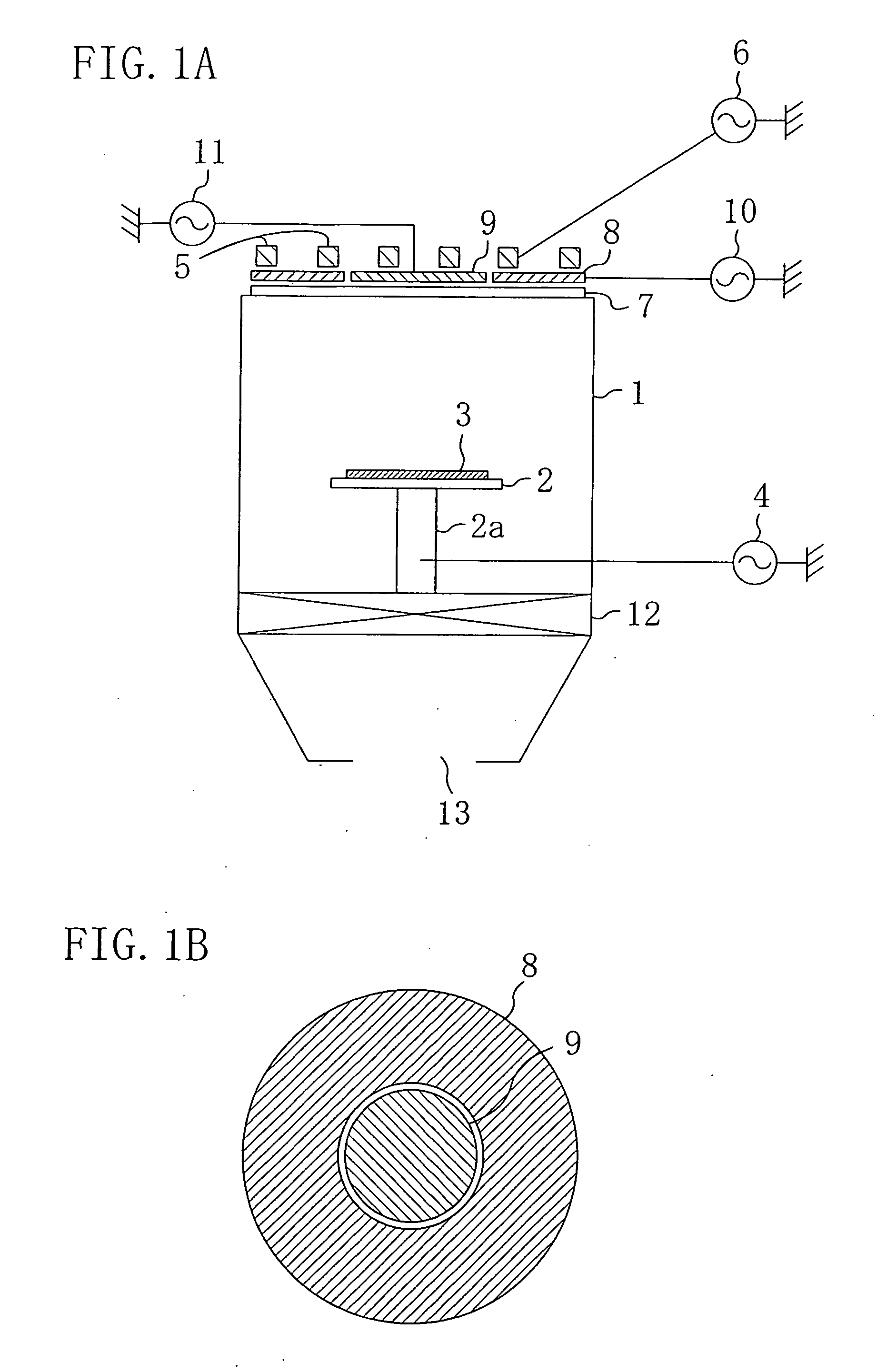
[0035] As explained above, according to the present invention, the second electrode such as a Faraday shield electrode comprises a plurality of separated electrodes and a high frequency voltage is applied independently to each of the separated electrodes based on the thickness distribution of the reaction product adhered to the chamber inner wall. Or alternatively, with the second electrode being moved along the chamber wall, a high frequency voltage is applied depending on the thickness of the reaction product adhered to a position to which the second electrode has been moved. Therefore, the reaction product remaining in the chamber is etched enough while part of the chamber inner wall immediately below the first electrode such as an ICP coil is prevented from being etched. Accordingly, particle generation derived from the reaction product is suppressed while exerting an original function of the second electrode, i.e., the waste of the insulating material forming the chamber is prevented with reliability. Thereby, the plasma etching of the electrode material film is carried out at low costs with fewer defects. In particular, in manufacturing an electrode of a ferroelectric memory, the present invention shows a remarkable effect if applied to the etching of a noble metal film or a platinum group metal film which gives a reaction product whose boiling point is too high for easy vaporization, i.e., a reaction product hard to exhaust out of the chamber.
[0036] That is, the present invention relates to a plasma etching apparatus and a plasma etching process and is particularly effective if applied to a manufacturing process including patterning of an electrode material film of a ferroelectric capacitor.

Problems solved by technology

Where the reaction product remains adhered to the insulating chamber inner wall in this way, there is caused a problem in that particles are generated inside the chamber 1 and fall onto the wafer 3 to cause defects.
Therefore, it is difficult to etch the reaction product enough by adjusting the voltage value applied to the FS electrode 40 during the etching.
This also brings about a problem of significant waste of the insulating material.

Method used


Image

  • Plasma ethching apparatus and plasma etching process
  • Plasma ethching apparatus and plasma etching process
  • Plasma ethching apparatus and plasma etching process

Examples


first embodiment

[0042] Hereinafter, an explanation is given to a plasma etching apparatus and a plasma etching process according to a first embodiment of the present invention with reference to the drawings.

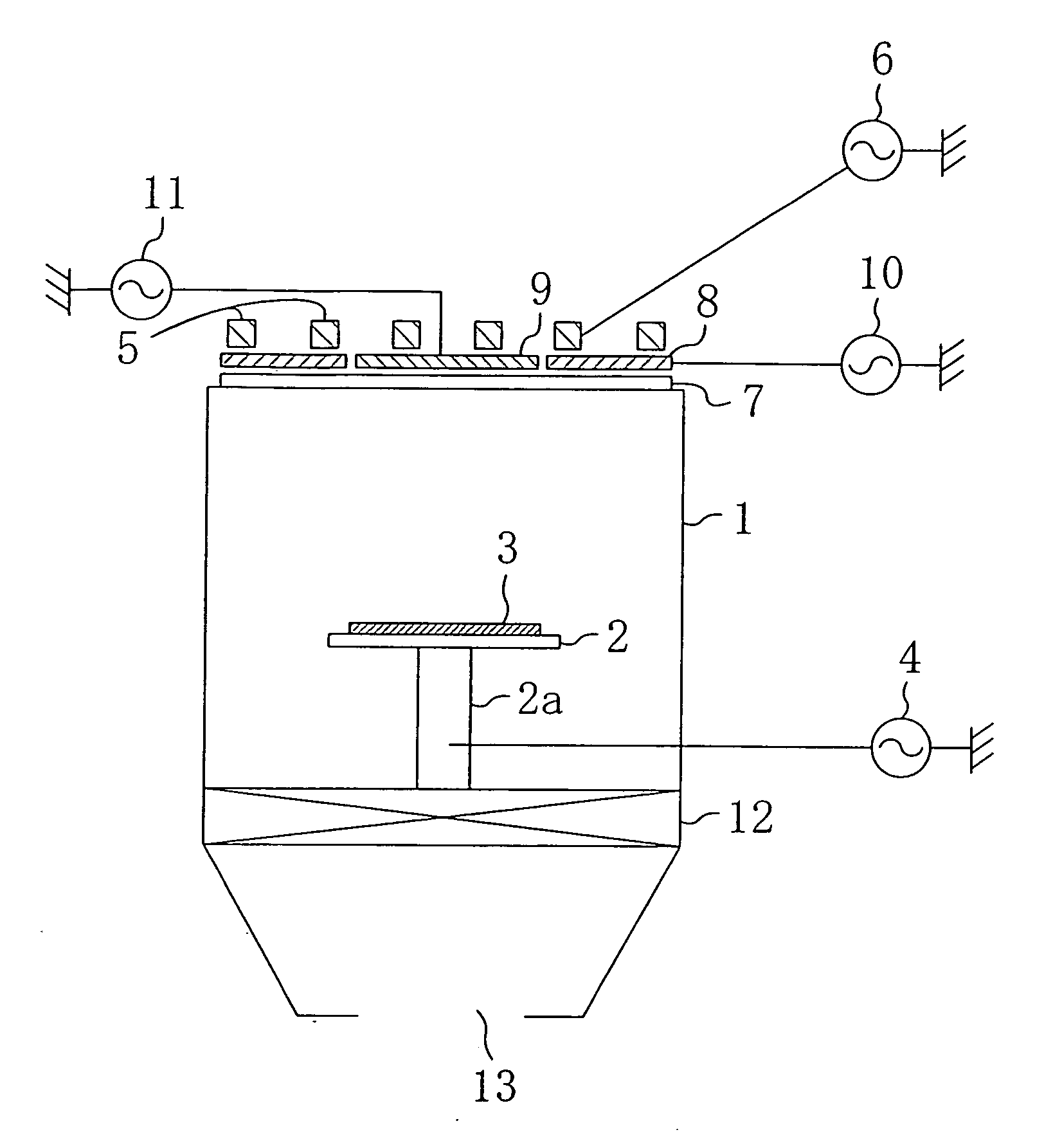
[0043]FIG. 1A is a view illustrating a schematic configuration of the plasma etching apparatus according to the first embodiment of the present invention. The plasma etching apparatus of the present embodiment allows generation of plasma which couples inductively with an ICP coil and plasma which couples capacitively with an FS electrode. As to be described later, a major feature of the apparatus is that the FS electrode is separated in two or more.

[0044] More specifically, as shown in FIG. 1A, the apparatus of the present embodiment includes an electrode 2 serving also as a wafer support arranged in a chamber 1 for performing plasma treatment such as dry etching, i.e., a chamber 1 capable of reducing pressure. The electrode 2 is installed on the bottom of the chamber 1 via a support member 2a...

second embodiment

[0065] Hereinafter, an explanation is given to a plasma etching apparatus and a plasma etching process according to a second embodiment of the present invention with reference to the drawings.

[0066]FIG. 4A is a view illustrating a schematic configuration of a plasma etching apparatus according to the second embodiment of the present invention. The plasma etching apparatus of the present embodiment allows generation of plasma which couples inductively with an ICP coil and plasma which couples capacitively with an FS electrode. Major features thereof are that the FS electrode moves in a creeping manner along a top plate at the top of a chamber 1 and that a device for monitoring in-situ a deposit adhered to the top plate (etching reaction product) is provided. That is, according to the etching process of the present invention, the etching is carried out while the step is repeated of specifying a position on the top plate where the reaction product is adhered by the in-situ monitoring ...


PUM

PropertyMeasurementUnit
boiling pointaaaaaaaaaa
sizeaaaaaaaaaa
frequencyaaaaaaaaaa

Abstract

A plasma etching apparatus includes: a chamber capable of reducing pressure; a substrate support provided inside the chamber to place a substrate; a first electrode which is arranged outside and in proximity to the chamber and to which high frequency power is applied to generate plasma of an etching gas in the chamber; and a second electrode comprising a plurality of separated electrodes which are arranged between the chamber and the first electrode and to each of which high frequency power is applied independently.

Description

CROSS-REFERENCE TO RELATED APPLICATIONS [0001] This non-provisional application claims priority under 35 U.S.C. § 119(a) on Patent Application No. 2004-066692 filed in Japan on Mar. 10, 2004, the entire contents of which are hereby incorporated by reference. BACKGROUND OF THE INVENTION [0002] (a) Field of the Invention [0003] The present invention relates to a plasma etching apparatus and a plasma etching process mainly used for patterning an electrode material film of a ferroelectric capacitor. In particular, the invention relates to a plasma etching apparatus for fine patterning of the electrode material film while suppressing particle generation and a plasma etching process using the same. [0004] (b) Description of Related Art [0005] With the increase in density, functionality and speed of semiconductor integrated circuit devices in recent years, techniques of using a nonvolatile memory (e.g., FeRAM (Ferroelectric Random Access Memory)) have been proposed. In the nonvolatile memo...

Claims


Application Information

Patent Timeline
Patent Type & Authority Applications(United States)
IPC IPC(8): C23F1/00H01L21/306H01L21/3065H01L21/8246H01L27/105
CPCC23F4/00H01J37/32091H01J37/321H01L21/32136H01L21/32139
Inventor OHKUNI, MITSUHIRO
Owner PANASONIC CORP
Learn More