Phase change memory devices with reduced programming current

a technology of phase change memory and programming current, which is applied in the direction of bulk negative resistance effect devices, semiconductor devices, electrical equipment, etc., can solve the problems of the number of masks required, and achieve the effect of reducing the required programming current, reducing the current density, and increasing the resistivity

Active Publication Date: 2007-04-05
TAIWAN SEMICON MFG CO LTD +1
View PDF11 Cites 94 Cited by
  • Summary
  • Abstract
  • Description
  • Claims
  • Application Information

AI Technical Summary

Benefits of technology

[0011] The preferred embodiment has several advantageous features. First, higher resistivity of the bottom electrode and top electrode help the concentration of the current and reduce the required programming current. Also, fewer errors occur due to reduced current density. Second, a higher ratio of the area of the bottom electrode to the top surface area of the conducting electrode reduces alloying of the bottom electrode with the phase change material. Third, the combination of lift-off technique and stacked layer design in some embodiments reduces the number of masks required for forming the phase change memory device.

Problems solved by technology

Third, the combination of lift-off technique and stacked layer design in some embodiments reduces the number of masks required for forming the phase change memory device.

Method used


Image

  • Phase change memory devices with reduced programming current
  • Phase change memory devices with reduced programming current
  • Phase change memory devices with reduced programming current

Examples


Embodiment Construction

[0018] The making and using of the presently preferred embodiments are discussed in detail below. It should be appreciated, however, that the present invention provides many applicable inventive concepts that can be embodied in a wide variety of specific contexts. The specific embodiments discussed are merely illustrative of specific ways to make and use the invention, and do not limit the scope of the invention.

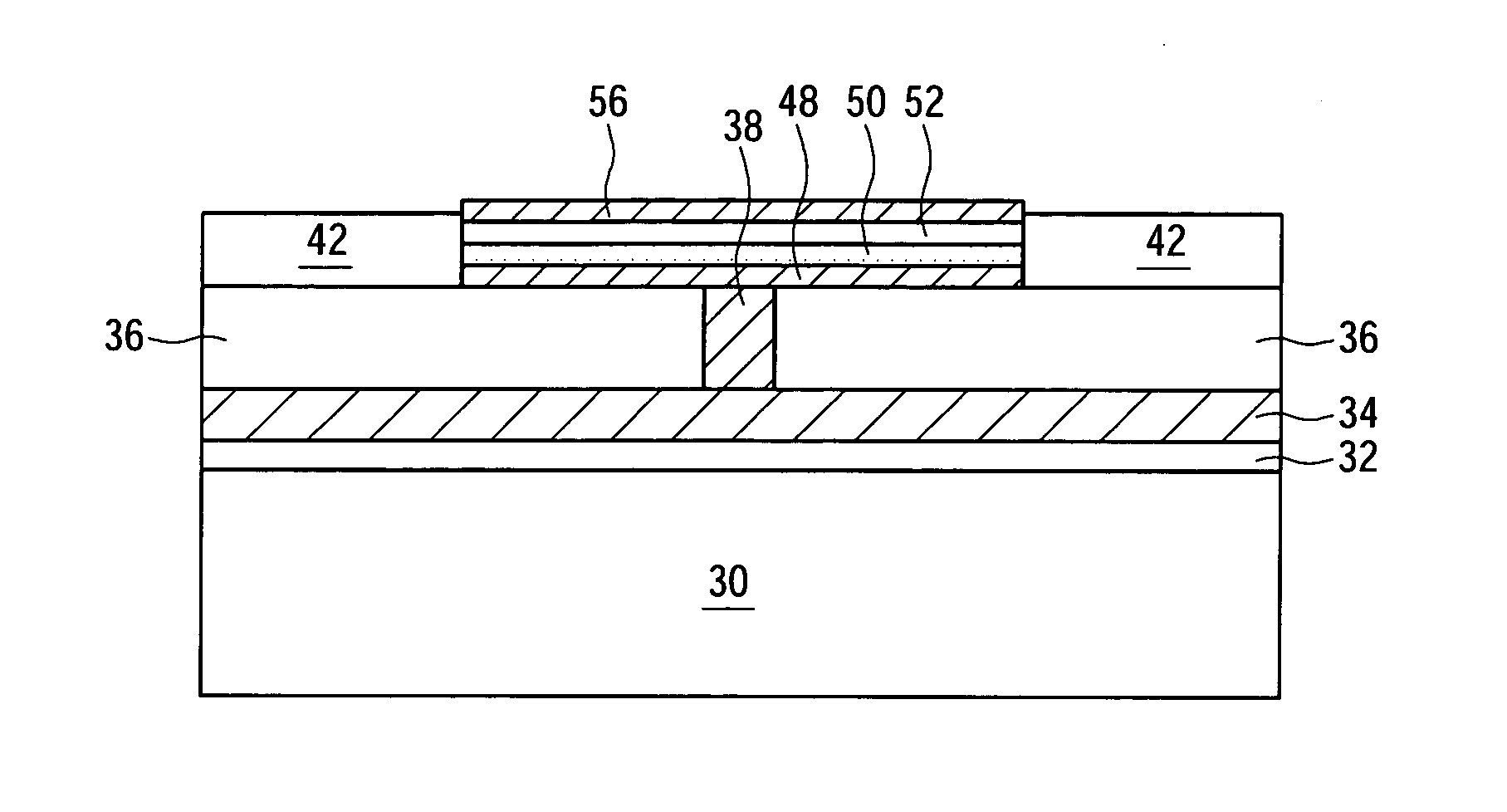
[0019] The intermediate stages of manufacturing a novel phase change memory device embodiment of the present invention are illustrated in FIGS. 4 through 7. Throughout the various views and illustrative embodiments of the present invention, like reference numbers are used to designate like elements.

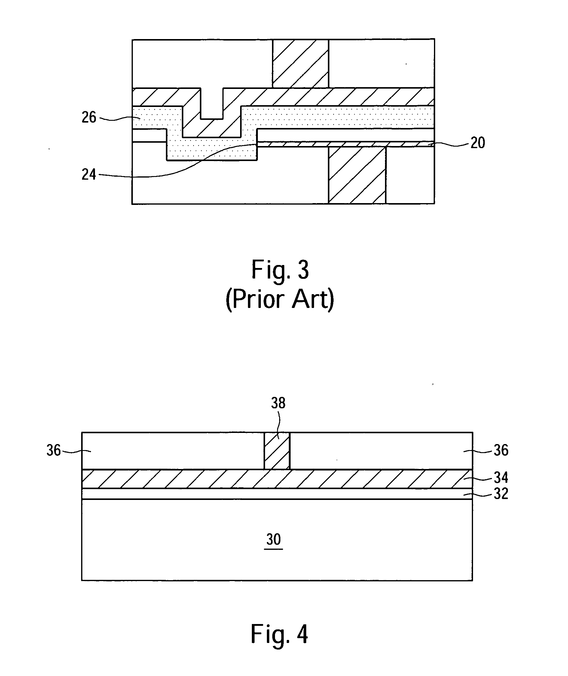
[0020]FIG. 4 illustrates a composite structure. An insulation layer 32 is formed over a substrate 30 and electrically insulates the memory structures that will be subsequently formed. Substrate 30 may be a silicon substrate or a substrate comprising other semiconductor materials...


PUM

PropertyMeasurementUnit
resistivityaaaaaaaaaa
thicknessesaaaaaaaaaa

Abstract

A phase change memory device and a method of forming the same are provided. The phase change memory device includes a conducting electrode in a dielectric layer, a bottom electrode over the conducting electrode, a phase change layer over the bottom electrode, and a top electrode over the phase change layer. The phase change memory device may further include a heat sink layer between the phase change layer and the top electrode. The resistivities of the bottom electrode and the top electrode are preferably greater than the resistivity of the phase change material in the crystalline state.

Description

[0001] This application claims priority to provisional patent application serial no. 60 / 660,794, filed Mar. 11, 2005, entitled “Phase Change Memory with Reduced Programming Circuit,” which application is incorporated herein by reference.TECHNICAL FIELD [0002] This invention relates generally to phase change memory devices, and more particularly to the structures and manufacturing methods of phase change memory devices having reduced programming current. BACKGROUND [0003] Phase change technology is promising for next generation memory devices. It uses chalcogenide semiconductors for storing states and digital information. The chalcogenide semiconductors, also called phase change materials, have a crystalline state and an amorphous state. In the crystalline state, the phase change materials have low resistivity; while in the amorphous state, they have high resistivity. The resistivity ratios of the phase change material in the amorphous and crystalline states are typically greater tha...

Claims


Application Information

Patent Timeline
Patent Type & Authority Applications(United States)
IPC IPC(8): H01L47/00H01L29/94H01L27/108H01L29/76H01L31/119
CPCH01L45/06H01L45/1233H01L45/126H01L45/144H01L45/128H01L45/1666H10N70/231H10N70/8413H10N70/861H10N70/826H10N70/8828H10N70/061
Inventor LAI, LI-SHYUETANG, DENNY DUAN-IEELIN, WEN-CHINYU, TENG-CHIENTSAI, HUI-FANGWANG, WEI-HSIANGWANG, SHYHYEU
Owner TAIWAN SEMICON MFG CO LTD
Why Eureka
Try Eureka