High performance device design

a high-performance, device technology, applied in the direction of semiconductor devices, basic electric elements, electrical equipment, etc., can solve the problems of complex formation process, high resistance, and drawbacks of vertical structures, so as to improve device drive current without the cost, increase the layout area, and increase the channel width

Active Publication Date: 2007-04-05
TAIWAN SEMICON MFG CO LTD
View PDF5 Cites 15 Cited by
  • Summary
  • Abstract
  • Description
  • Claims
  • Application Information

AI Technical Summary

Benefits of technology

[0009] By forming a recess in the active region, the channel width is increased and device drive current is improved without the cost of increased layout area.

Problems solved by technology

Vertical structures, however, suffer drawbacks.
The high resistance is an inherent limitation for further improving FinFET transistor performance.
Additonally, formation processes are complex due to difficulties caused by a high aspect ratio in manufacturing steps such as etching, implanting, and lithography, etc.

Method used


Image

  • High performance device design
  • High performance device design
  • High performance device design

Examples


Embodiment Construction

[0017] The making and using of the presently preferred embodiments are discussed in detail below. It should be appreciated, however, that the present invention provides many applicable inventive concepts that can be embodied in a wide variety of specific contexts. The specific embodiments discussed are merely illustrative of specific ways to make and use the invention, and do not limit the scope of the invention.

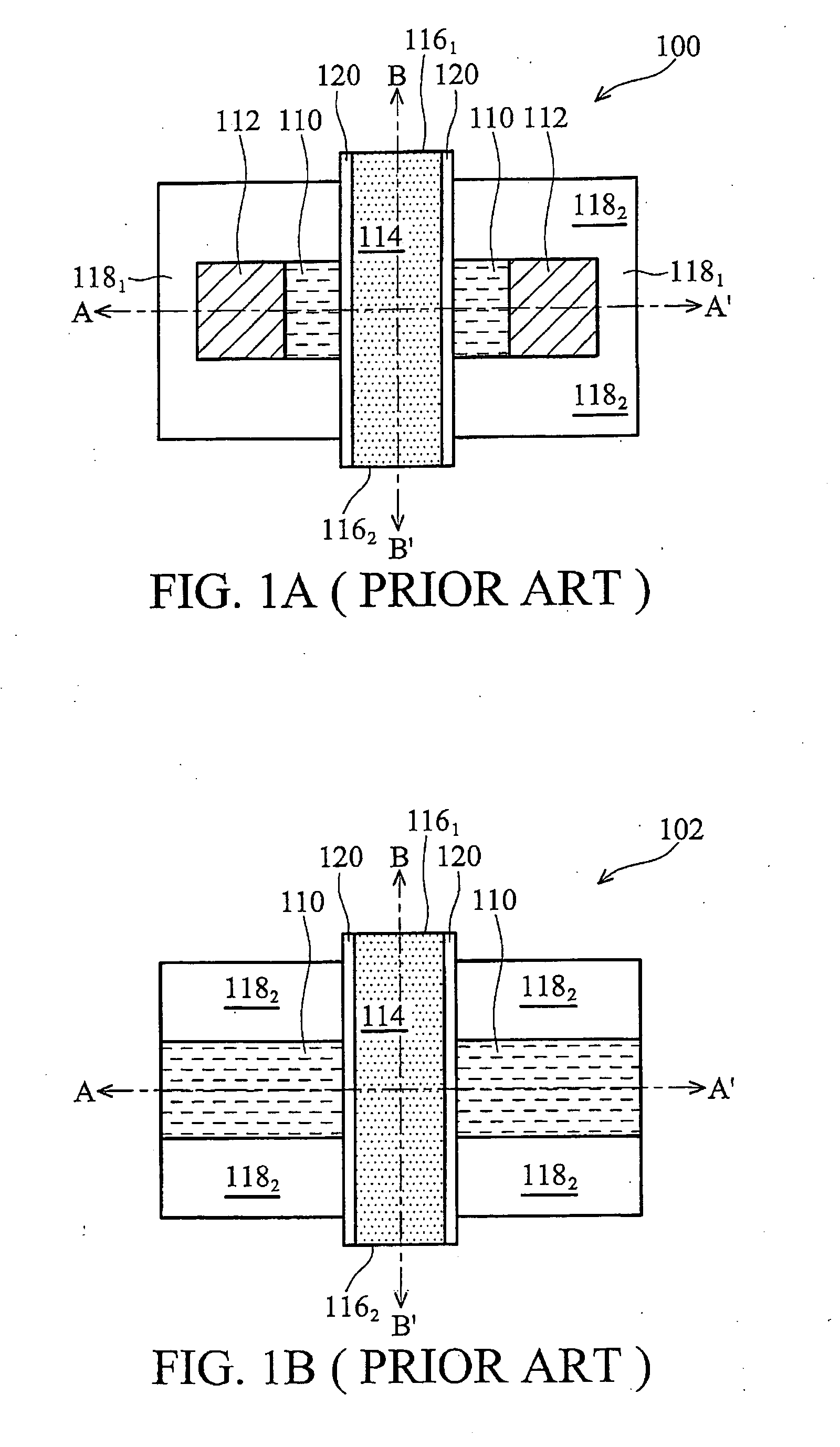
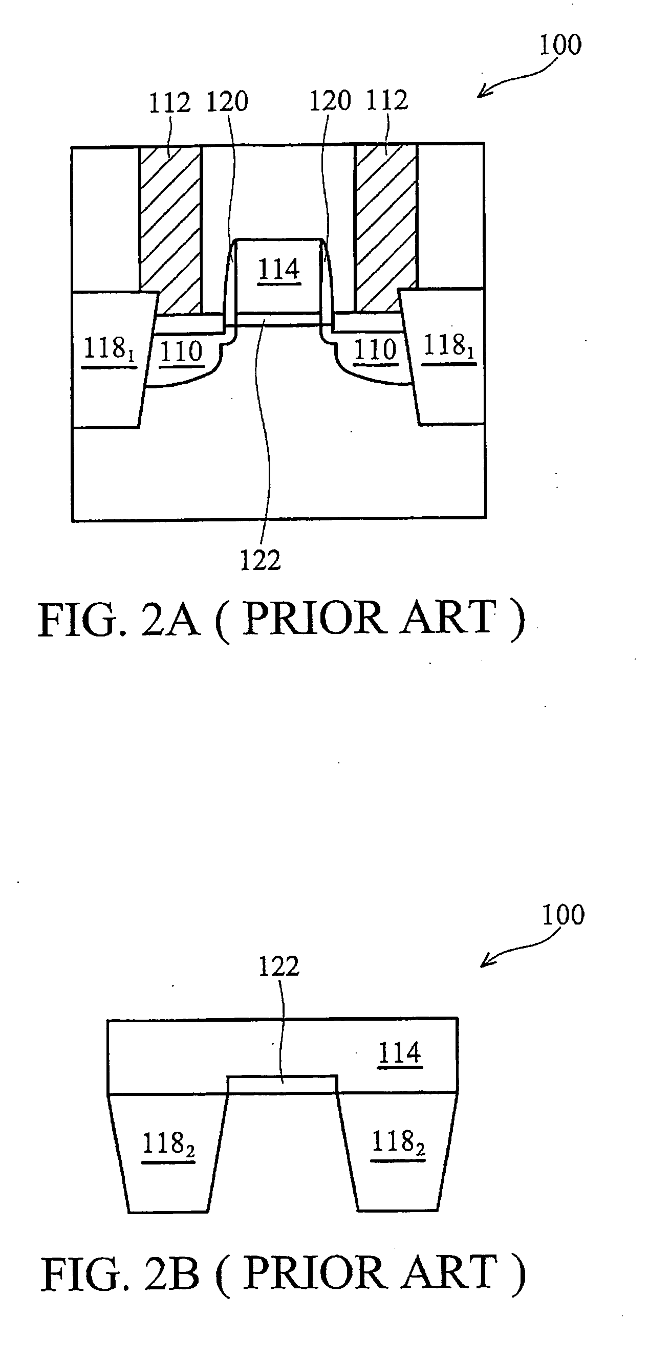
[0018] A novel method of forming a MOS device is provided. Throughout the various views and illustrative embodiments of the present invention, like reference numbers are used to designate like elements. FIGS. 1A and 1B illustrate schematic layouts of MOS devices 100 and 102, respectively. MOS devices 100 and 102 have similar structures except their source / drains are connected to other components of the integrated circuit in different ways. Each of the transistors 100 and 102 includes source / drain regions (active areas) 110, a gate electrode 114, and gate spacers 120. Gate e...


PUM


Abstract

A semiconductor structure having a recessed active region and a method for forming the same are provided. The semiconductor structure comprises a first and a second isolation structure having an active region therebetween. The first and second isolation structures have sidewalls with a tilt angle of substantially less than 90 degrees. The active region is recessed. By recessing the active region, the channel width is increased and device drive current is improved.

Description

TECHNICAL FIELD [0001] This invention relates generally to semiconductor devices, and particularly to manufacturing processes of semiconductor devices, and more particularly to the formation of shallow trench isolations and active regions. BACKGROUND [0002] Shallow trench isolation (STI) has been the most widely used isolation structure for sub 0.25 μm CMOS generation and beyond due to its good scalability and isolation performance. The main process steps of STI, i.e., dry etching silicon for trench formation and oxide gap-filling the trench, significantly impact device performance and reliability. As transistors are continuously scaled down, the electrical behavior of narrow width transistors is influenced more significantly by STI corner profiles and manufacturing processes than that of wide width transistors. [0003] Among promising structures that have improved device performance and reliability, vertical structures, such as FinFETs, have excellent short channel control and incre...

Claims


Application Information

Patent Timeline
Patent Type & Authority Applications(United States)
IPC IPC(8): H01L29/76
CPCH01L21/823412H01L21/823481H01L29/1037
Inventor HUANG, CHIEN-CHAOYANG, FU-LIANG
Owner TAIWAN SEMICON MFG CO LTD
Why Eureka
Try Eureka