Semiconductor chip and semiconductor device

Active Publication Date: 2007-04-05
SHARP KK
View PDF8 Cites 4 Cited by
  • Summary
  • Abstract
  • Description
  • Claims
  • Application Information

AI Technical Summary

Benefits of technology

[0023] According to the arrangement, since there is no need to design a dedicated semiconductor chip separately, production cost can be reduced. Further, from among the first and second electrode sections which are electrically connected to each other, the first electrode section disposed in the peripheral part of the semiconductor chip can be used for performing wire bonding. This enables the wire to have shorter length, compared to a case wher

Problems solved by technology

However, with such conventional wafer level CSP techniques, disposing external connection terminals in the peripheral part as well as in the vicinity of the center part of the semiconductor chip causes a problem of being unable to draw wires from the electrode pads to the external connection terminals in the vicinity of the center part.
As

Method used


Image

  • Semiconductor chip and semiconductor device
  • Semiconductor chip and semiconductor device
  • Semiconductor chip and semiconductor device

Examples


Embodiment Construction

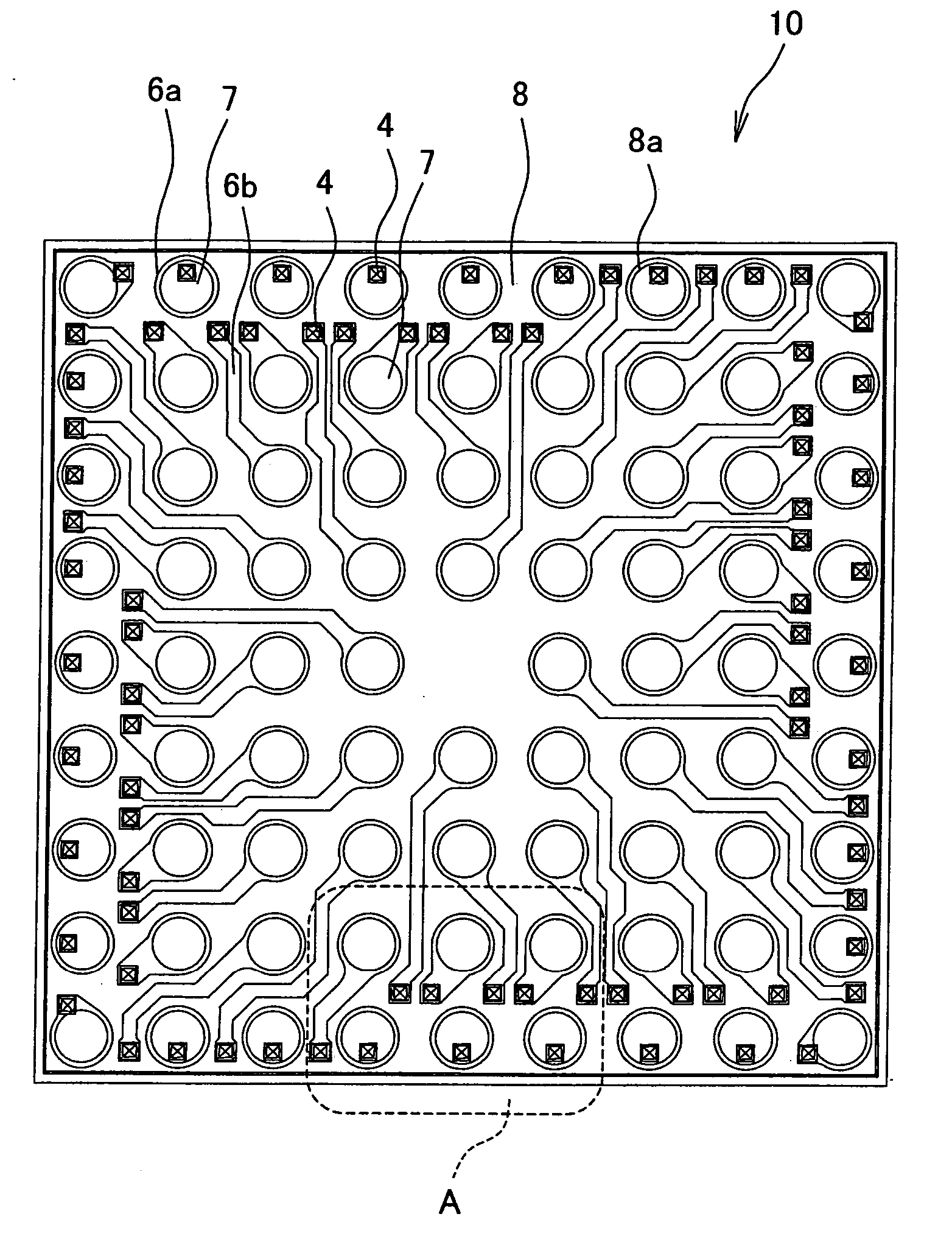
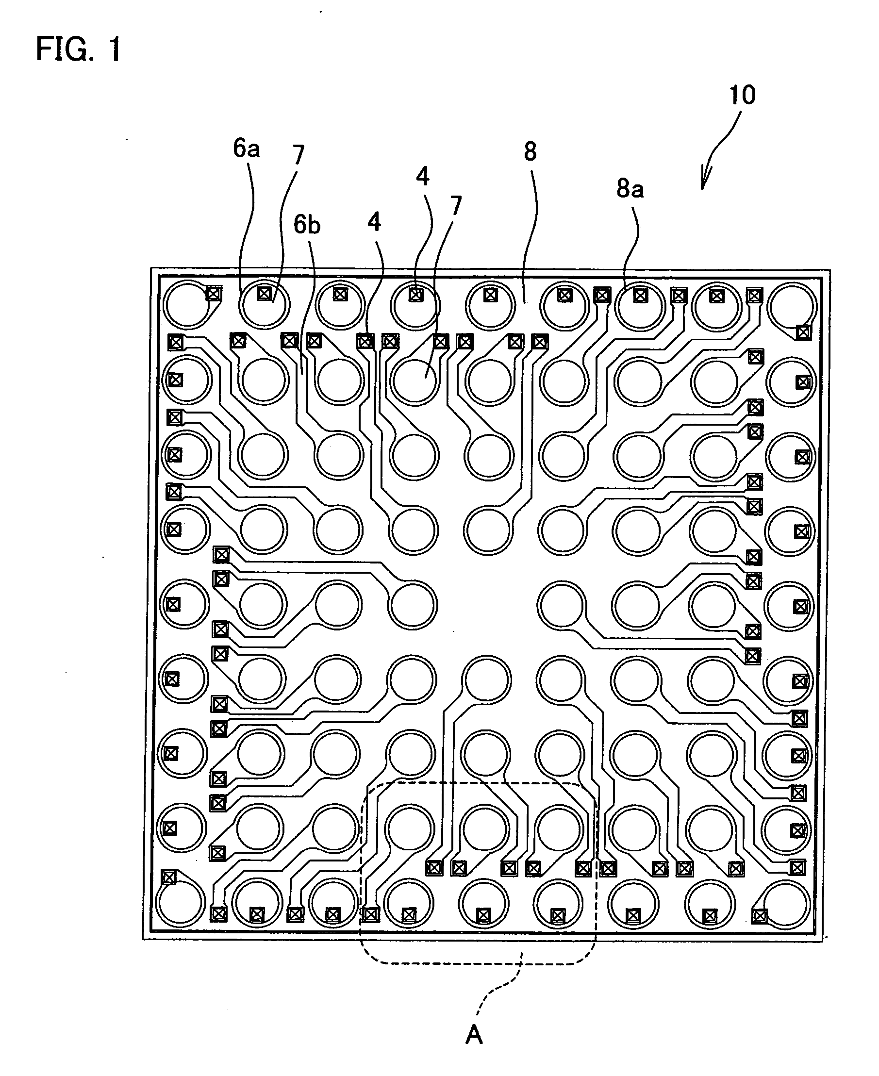
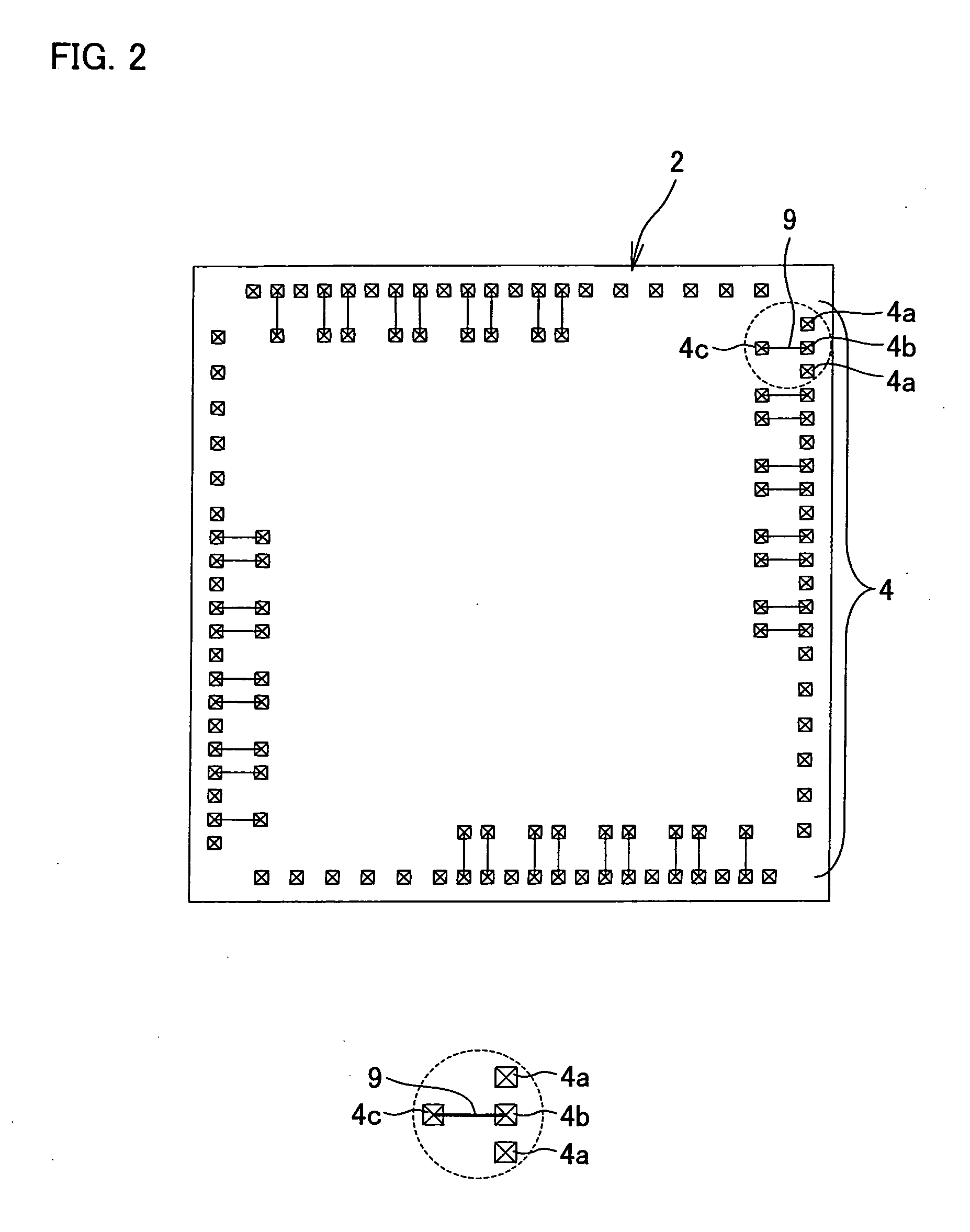
[0032] The following will describe one embodiment of the present invention. FIG. 2 is a plan view illustrating a schematic structure of a main surface of a semiconductor chip 2 according to the present embodiment (surface on which a semiconductor element (semiconductor integrated circuit) is provided). In FIG. 2, an arrangement of electrode pads (electrode sections) 4 is mainly illustrated.

[0033] The semiconductor chip 2 of the present embodiment has external connection terminals 7 mounted thereon. The semiconductor chip 2 can be applied to (i) a wafer level CSP in which the semiconductor chip 2 itself serves as a semiconductor package, and (ii) a semiconductor package (CSP etc.) in which the semiconductor chip 2 is electrically connected to a stacked substrate by wire bonding.

[0034] As shown in FIG. 2, the semiconductor chip 2 has (i) a large number of electrode pads 4 (4a and 4b) disposed along the peripheral part of its main surface, and (ii) a large number of electrode pads 4 ...


PUM


Abstract

In the peripheral part of a semiconductor chip, third electrode pads for wire bonding and plate wiring and first electrode pads dedicated to wire bonding are provided. On the other hand, second electrode pads dedicated to plate wiring are provided on an inner part away from the edge of the semiconductor chip. Further, the first and second electrode pads are connected via metal bypass layers, respectively. In the case of wire bonding, the first and third electrode pads are used and the third electrode pads are encapsulated with an insulating layer. Further, in the case of plate wiring, the second and third electrode pads are used and the first electrode pads are covered with an insulating layer. This realizes a semiconductor chip which has great versatility and which can be used in semiconductor packages of various types.

Description

[0001] This Nonprovisional application claims priority under 35 U.S.C. § 119(a) on Patent Application No. 289429 / 2005 filed in Japan on Sep. 30, 2005, the entire contents of which are hereby incorporated by reference. FIELD OF THE INVENTION [0002] The present invention relates to (i) a semiconductor chip which is mounted on or built in an electronic device, and(ii) a semiconductor package (semiconductor device) containing the semiconductor chip. BACKGROUND OF THE INVENTION [0003] In recent years, particularly in the field of small-sized portable electronic devices, there has been a movement toward downsizing, high functionality, and high-density mounting of electronic components, which are built in electronic devices. According to such a movement, there has been a demand for small-sized semiconductor packages which contain semiconductor chips. [0004] One example of such small-sized semiconductor packages is a semiconductor package being equal in size to a chip (CSP: Chip Size Packag...

Claims


Application Information

Patent Timeline
IPC IPC(8): H01L23/48
CPCH01L23/3114H01L24/13H01L24/05H01L24/06H01L24/10H01L24/45H01L24/48H01L24/85H01L2224/0401H01L2224/04042H01L2224/05556H01L2224/13099H01L2224/16H01L2224/45144H01L2224/48227H01L2224/48465H01L2224/48599H01L2224/49175H01L2924/01004H01L2924/01005H01L2924/01013H01L2924/01014H01L2924/01022H01L2924/01029H01L2924/0105H01L2924/01074H01L2924/01078H01L2924/01079H01L2924/01082H01L2924/014H01L2924/05042H01L2924/14H01L2924/15311H01L23/525H01L2224/73265H01L2924/01006H01L2924/01024H01L2924/01033H01L2924/01055H01L24/49H01L2224/85H01L2224/32225H01L2924/00014H01L2924/00H01L2924/00012H01L2224/023H01L2224/05554H01L2224/05624H01L2224/13H01L2924/10162H01L2924/181H01L2924/0001
Inventor NAKANISHI, HIROYUKIMORI, HARUYA
Owner SHARP KK
Why Eureka
Try Eureka