

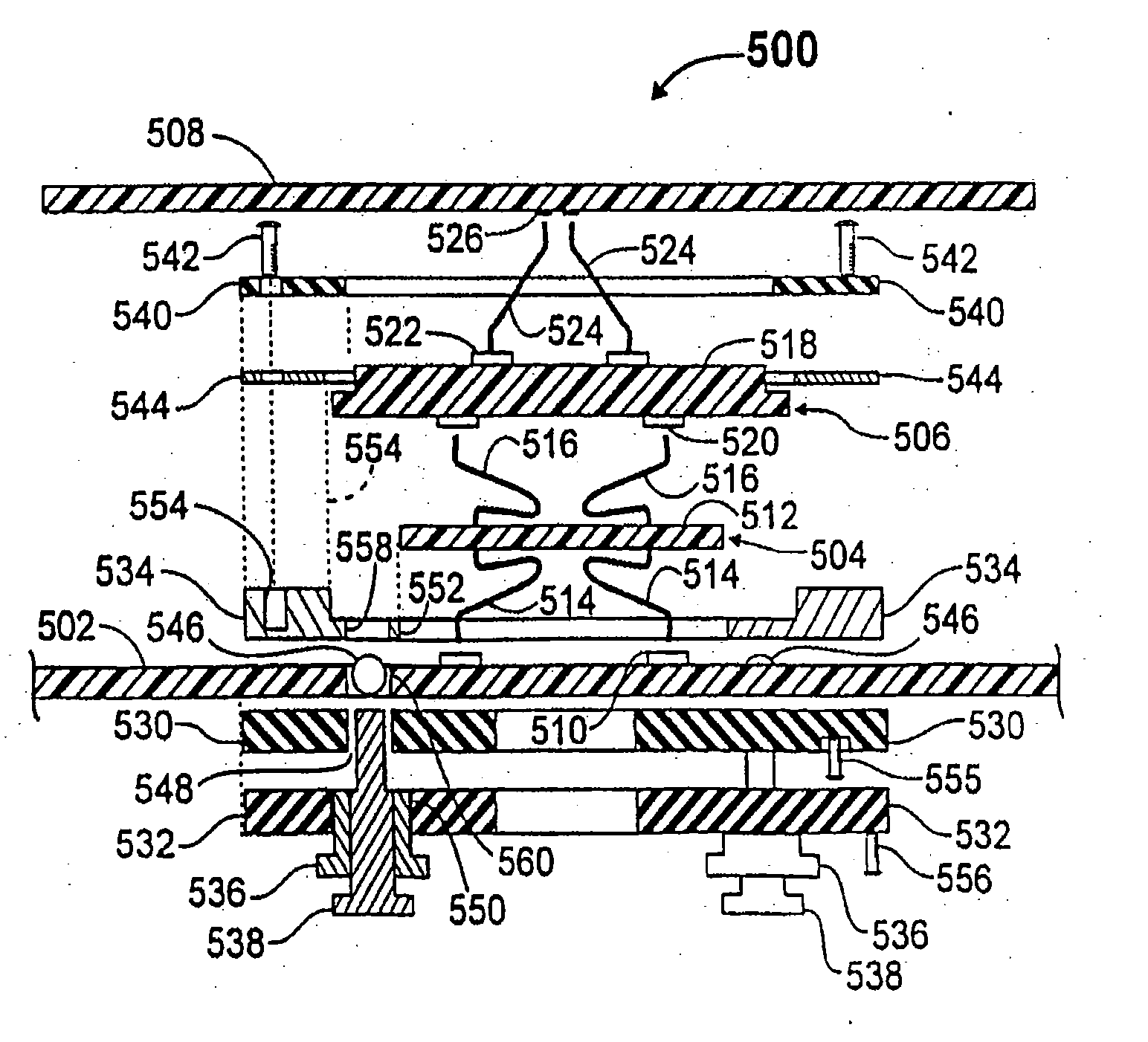
Contact Carriers (Tiles) For Populating Larger Substrates With Spring Contacts
a technology of contact carriers and spring contacts, which is applied in the field of contact carriers, can solve the problems of dies being “bad” (non-functional), dies being “good” (full functional), and certain difficulties inherent in any technique for probing semiconductor dies, etc., and achieves the effects of easy rework, easy mounting, and easy testing and/or burning
- Summary
- Abstract
- Description
- Claims
- Application Information
AI Technical Summary
Benefits of technology
Problems solved by technology
Method used
Image

Examples
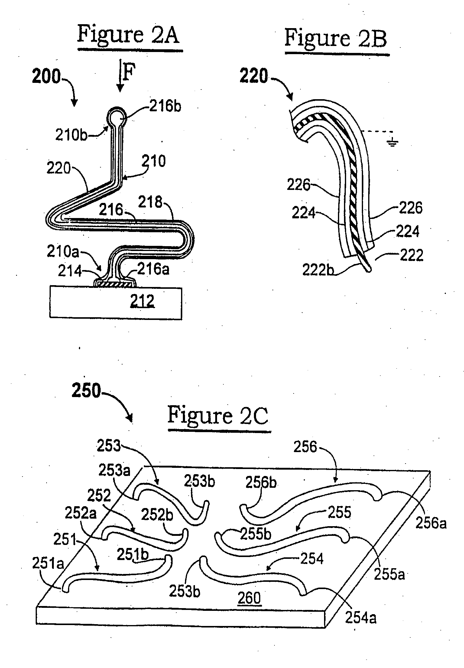
embodiment 200
[0152]FIG. 2A illustrates an embodiment 200 of an interconnection element 210 mounted to a terminal 214 of an electronic component 212. In this example, a soft (e.g., gold) wire core 216 is bonded (attached) at one end 216a to the terminal 214, is configured to extend from the terminal and have a spring shape (compare the shape shown in FIG. 1B), and is severed to have a free end 216b. Bonding, shaping and severing a wire in this manner is accomplished using wirebonding equipment. The bond at the end 216a of the core covers only a relatively small portion of the exposed surface of the terminal 214.
[0153] A shell (overcoat) is disposed over the wire core 216 which, in this example, is shown as being multi-layered, having an inner layer 218 and an outer layer 220, both of which layers may suitably be applied by plating processes. One or more layers of the multi-layer shell is (are) formed of a hard material (such as nickel and its alloys) to impart a desired resiliency to the intercon...
embodiment 250
[0169]FIG. 2C illustrates an embodiment 250 wherein a plurality (six of many shown) of interconnection elements 251 . . . 256 are mounted on a surface of an electronic component 260, such as a probe card insert (a subassembly mounted in a conventional manner to a probe card). Terminals and conductive traces of the probe card insert are omitted from this view, for illustrative clarity. The attached ends 251a . . . 256a of the interconnection elements 251 . . . 256 originate at a first pitch (spacing), such as 0.05-0.10 inches. The interconnection elements 251 . . . 256 are shaped and / or oriented so that their free ends (tips) are at a second, finer pitch, such as 0.005-0.010 inches. An interconnect assembly which makes interconnections from a one pitch to another pitch is typically referred to as a “space transformer”.
[0170] As illustrated, the tips 251b . . . 256b of the interconnection elements are arranged in two parallel rows, such as for making contact to (for testing and / or bur...
embodiment 270
[0185]FIG. 2I illustrates an alternate embodiment 270 for fabricating interconnection elements. In this embodiment, a masking material 272 is applied to the surface of a sacrificial substrate 274, and is patterned to have a plurality (one of many shown) of openings 276, in a manner similar to the technique described hereinabove with respect to FIG. 2D. The openings 276 define areas whereat interconnection elements will be fabricated as free-standing structures. (As used throughout the descriptions set forth herein, an interconnection element is “free-standing” when is has a one end bonded to a terminal of an electronic component or to an area of a sacrificial substrate, and the opposite end of the interconnection element is not bonded to the electronic component or sacrificial substrate.)
[0186] The area within the opening may be textured, in any suitable manner, such as to have one or more depressions, as indicated by the single depression 278 extending into the surface of the sacri...
PUM
| Property | Measurement | Unit |
|---|---|---|
| length | aaaaa | aaaaa |
| length | aaaaa | aaaaa |
| diameter | aaaaa | aaaaa |
Abstract
Description
Claims
Application Information