Wiring board and capacitor

a technology of wiring board and capacitor, which is applied in the direction of structural fixed capacitor combination, cross-talk/noise/interference reduction, and association of printed circuit non-printed electric components, etc. it can solve the problems of not being able to omit the mounting process of inductors, affecting the effect of manufacturing steps, and unable to achieve low cost. achieve the effect of fine adjustment of capacitance value and preventing an increase in the number of manufacturing steps

Active Publication Date: 2007-04-05
NGK SPARK PLUG CO LTD
View PDF8 Cites 60 Cited by
  • Summary
  • Abstract
  • Description
  • Claims
  • Application Information

AI Technical Summary

Benefits of technology

[0033] Also, the aforementioned capacitor may be formed on at least one of the capacitor main surface and the capacitor reverse surface. The capacitor formed at such a position is exposed on the outer surface of the capacitor, so that this arrangement is advantageous in that trimming and the like can be provided after the forming, making it possible to finely adjust the capacitance value.
[0034] Alternatively, the aforementioned capacitor may be formed in the interior of the capacit

Problems solved by technology

Hence, even if the multifunction can be attained, it has been difficult to attain a further compact size.
In addition, in the manufacture of such package

Method used


Image

  • Wiring board and capacitor
  • Wiring board and capacitor
  • Wiring board and capacitor

Examples


first embodiment

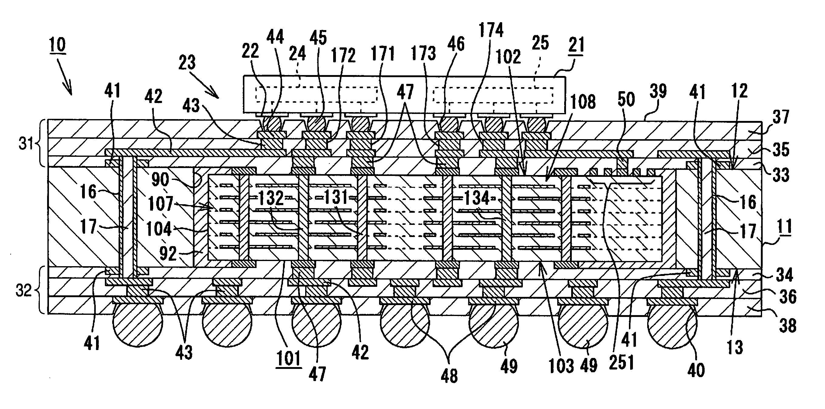
[0141] Referring now to the drawings, a detailed description will be given of a first embodiment of the wiring board in accordance with the invention.

[0142] As shown in FIGS. 1 and 23, a wiring board 10 or 110 in accordance with this embodiment is comprised of a substantially rectangular plate-shaped board core 11 which is a wiring board for mounting on an IC chip and is formed of glass epoxy; a first buildup layer 31 (wiring laminated portion) formed on an upper surface 12 (core main surface) of the board core 11; and a second buildup layer 32 formed on a lower surface 13 (core reverse surface) of the board core 11. Through hole conductors 16 are formed at a plurality of portions in the board core 11. These through hole conductors 16 connect and conduct the upper surface 12 side and the lower surface 13 side of the board core 11. It should be noted that the interior of each through hole conductor 16 is filled with a closure body 17 such as an epoxy resin. Further, conductor layers...

second embodiment

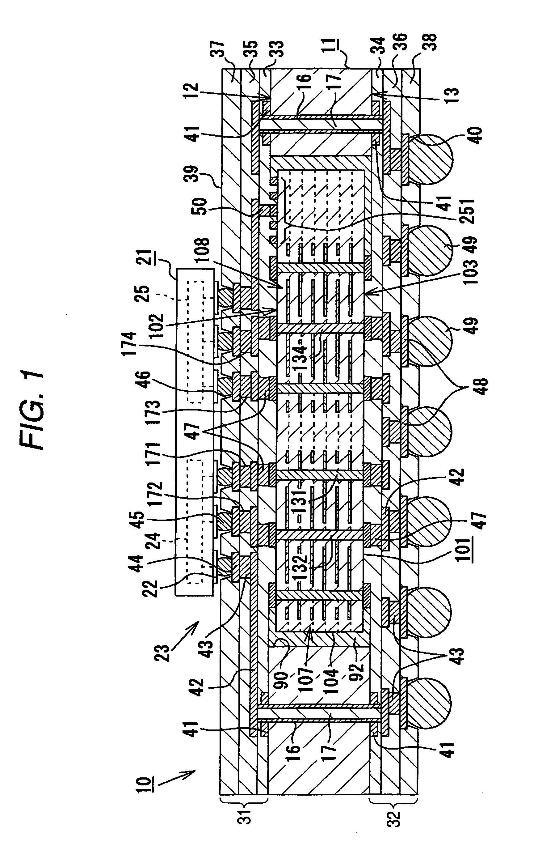
[0190] Referring now to FIGS. 9 to 12, a detailed description will be given of the ceramic capacitor in accordance with a second embodiment of the invention.

[0191] A ceramic capacitor 101A in accordance with this embodiment shown in FIGS. 9 and 10 has the obverse surface-side inductor pattern 251 serving as an inductor in the same way as in the first embodiment. This obverse surface-side inductor pattern 251 is disposed in a region located outside the capacitor function portions 107 and 108 on the upper surface 102 of the ceramic capacitor 101A. An obverse surface-side resistor pattern 261 serving as a resistor is formed in that region in the vicinity of the obverse surface-side inductor pattern 251. The obverse surface-side resistor pattern 261 in this embodiment is a rectilinear pattern, but may be a meandering linear pattern. A via conductor 281 for a signal line providing communication between the upper surface 102 and the lower surface 103 of the ceramic capacitor 101A is disp...

third embodiment

[0194] Referring now to FIG. 13, a detailed description will be given of the ceramic capacitor in accordance with a third embodiment of the invention.

[0195] In the second embodiment, one circuit portion 300 or 300A (filter circuit) is formed on the upper surface 102 of the ceramic capacitor 101. In contrast, in this embodiment shown in FIG. 13, two circuit portions 300B (filter circuits) are formed inside a ceramic capacitor 101B. Specifically, a resistor constituting the circuit portion 300B is an inner layer resistor pattern 263. One end of the inner layer resistor pattern 263 is electrically connected to a predetermined terminal portion 285 located on the surface layer through an interlayer-connecting via conductor 267. A loop-shaped inner layer inductor pattern 253 is formed in a layer underneath the layer where the inner layer resistor pattern 263 is formed. An outer end of the inner layer inductor pattern 253 is electrically connected to the remaining end of the inner layer r...


PUM


Abstract

A wiring board comprising: a board core (11) having a core main surface (12) and a core reverse surface (13); a capacitor (101, 101A, 101B, 101C, 101D, 101E, 101F, 101G, 101H, 101J, 1101, 1101′, 1101″, 1101′″, 1101″″, 1101′″″) having a capacitor main surface (102) and a capacitor reverse surface (103) and having a structure in which first inner electrode layers (141) and second inner electrode layers (142) are alternately laminated and arranged via a dielectric layer (105), the capacitor (101, 101A, 101B, 101C, 101D, 101E, 101F, 101G, 101H, 101J, 1101, 1101′, 1101″, 1101′″, 1101″″, 1101′″″) being accommodated in the board core (11) in a state in which the core main surface (12) and the capacitor main surface (102) are oriented on a same side; and a wiring laminated portion (31) having a structure in which interlayer insulating layers (33, 35) and conductor layers (42) are alternately laminated on the core main surface (12) and the capacitor main surface (102), wherein an inductor (251, 252, 253) or a resistor (301, 302, 311, 312, 321, 322) is formed on or in the capacitor (101, 101A, 101B, 101C, 101D, 101E, 101F, 101G, 101H, 101J, 1101, 1101′, 1101″, 1101′″, 1101″″, 1101′″″).

Description

FIELD OF THE INVENTION [0001] The present invention relates to a wiring board having a structure in which a capacitor mainly consisting of a ceramic and the like is embedded in a board core, a wiring laminated layer is formed by being laminated on its surface, and a semiconductor integrated circuit device is mounted thereon, as well as a capacitor used on the wiring board. BACKGROUND OF THE INVENTION [0002] Semiconductor integrated circuit devices (IC chips) used in such as microprocessors and chip sets of computers in recent years tend to be characterized by increasingly higher speed and higher functions, and the number of terminals tends to increase and the pitch between the terminals tends to become narrower correspondingly. Generally, a multiplicity of terminals are densely arranged in array form on the bottom surface of the IC chip, and such terminal groups are connected to terminal groups on the motherboard side in flip chip form. However, since there is a large difference in ...

Claims


Application Information

Patent Timeline
IPC IPC(8): H05K1/18
CPCH01G2/06H01L2224/16235H01L21/568H01L21/6835H01L23/49822H01L23/49838H01L24/81H01L2221/68345H01L2224/16225H01L2224/81192H01L2224/81801H01L2924/01013H01L2924/01029H01L2924/01033H01L2924/01038H01L2924/01056H01L2924/01078H01L2924/01082H01L2924/09701H01L2924/14H01L2924/15311H01L2924/19041H01L2924/19042H01L2924/19043H01L2924/30105H01L2924/30107H05K1/0233H05K1/0234H05K1/185H05K3/4602H05K2201/10045H05K2201/10674H05K2201/10712H01L2924/01005H01L2924/01006H01L2924/01019H01L2924/01042H01L2924/01047H01L2924/01074H01L2924/014H01G4/40H01L2224/05568H01L2224/05573H01L2924/00014H01L2924/12042H01L2924/351H01L2924/00H01L2224/05599
Inventor URASHIMA, KAZUHIROYURI, SHINJISATO, MANABUOGAWA, KOHKI
Owner NGK SPARK PLUG CO LTD
Why Eureka
Try Eureka