Electrophotographic photoconductor and manufacturing method of electrophotographic photoconductor

a manufacturing method and photoconductor technology, applied in the field of electrophotographic photoconductor and electrophotographic photoconductor manufacturing method, can solve the problems of poor initial sensitivity, poor durability, and difficulty in using charge transferring agent having the average molecular weight outside the range, and achieve easy and stably formation, enhance the preservation stability of coating solution for forming an intermediate layer, and efficiently manufacture the electrophotographic photoconductor

Inactive Publication Date: 2007-04-05
KYOCERA DOCUMENT SOLUTIONS INC
View PDF7 Cites 15 Cited by
  • Summary
  • Abstract
  • Description
  • Claims
  • Application Information

AI Technical Summary

Benefits of technology

[0016] Accordingly, inventors of the present invention have extensively studied these drawbacks and as a result of the studies, the inventors have found out that in an electrophotographic photoconductor which includes a support base body, an intermediate layer and a photoconductor layer, by allowing the intermediate layer to contain titanium oxide and a binding resin and by setting a whiteness of the intermediate layer (ΔL value) which is measured by a color-difference meter in accordance with JIS Z 8722 to a value which falls within a predetermined range or by setting a reflection absorbance (ΔA value) to a value which falls within a predetermined range, even when a surrounding environmental condition is changed, the electrophotographic photoconductor can obtain the excellent image properties.
[0043] Due to such a manufacturing method, the preservation stability of the coating solution for forming a intermediate layer is enhanced and hence, it is possible to easily and stably form the predetermined intermediate layer and, at the same time, it is possible to efficiently manufacture the electrophotographic photoconductor which can reduce the generation of fogging under a high-temperature and high-moisture condition.

Problems solved by technology

However, in the image forming apparatus which includes the electrophotographic photoconductor having the intermediate layer described in patent document 1 has a drawback that the intermediate layer is formed by using the electron transferring organic pigment and hence, the electrophotographic photoconductor exhibits poor initial sensitivity and also exhibits poor durability.
Further, although the electrophotographic photoconductor having the intermediate layer which is described in patent document 2 exhibits the excellent electric properties and the excellent image properties, an average molecular weight of a usable charge transferring agent is limited to a range from 400 to 1000 and hence, there has been a drawback that it is difficult to use the charge transferring agent having the average molecular weight outside the range.
Further, the electrophotographic photoconductors which are described in patent document 1 and patent document 2 use a large quantity of a thermosetting phenol-based resin and hence, the color of the electrophotographic photoconductor is liable to be easily faded or made thick thus giving rise to a drawback that it is difficult to determine the uniformity of the thickness or the like in the intermediate layer by using an optical method.

Method used


Image

  • Electrophotographic photoconductor and manufacturing method of electrophotographic photoconductor
  • Electrophotographic photoconductor and manufacturing method of electrophotographic photoconductor
  • Electrophotographic photoconductor and manufacturing method of electrophotographic photoconductor

Examples


first embodiment

[First Embodiment]

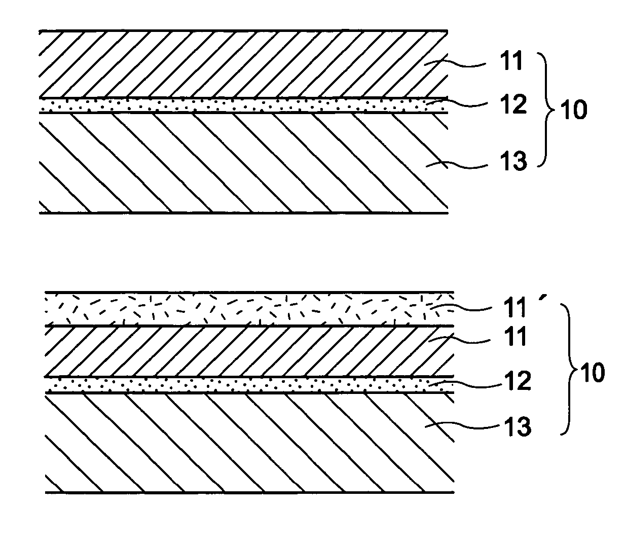
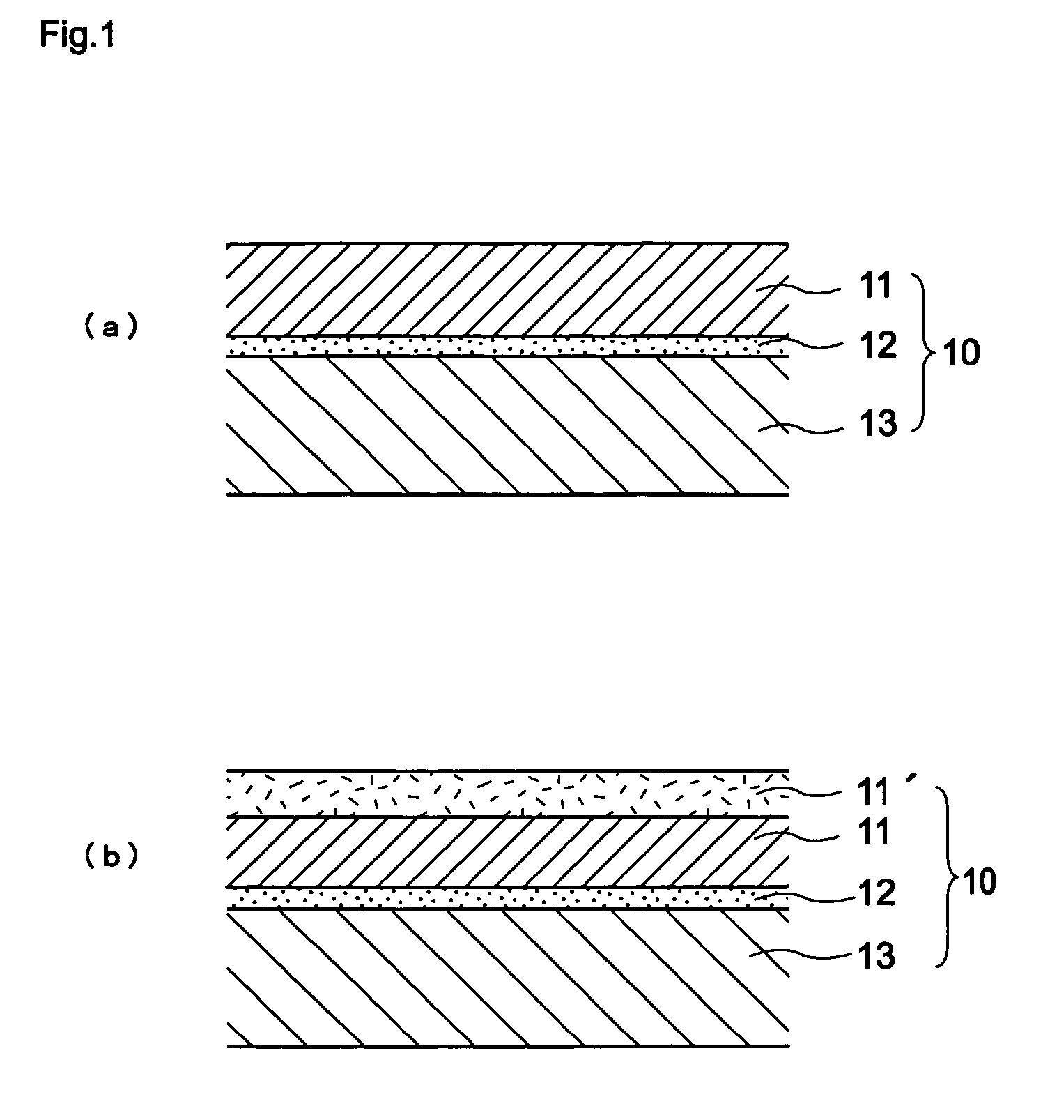
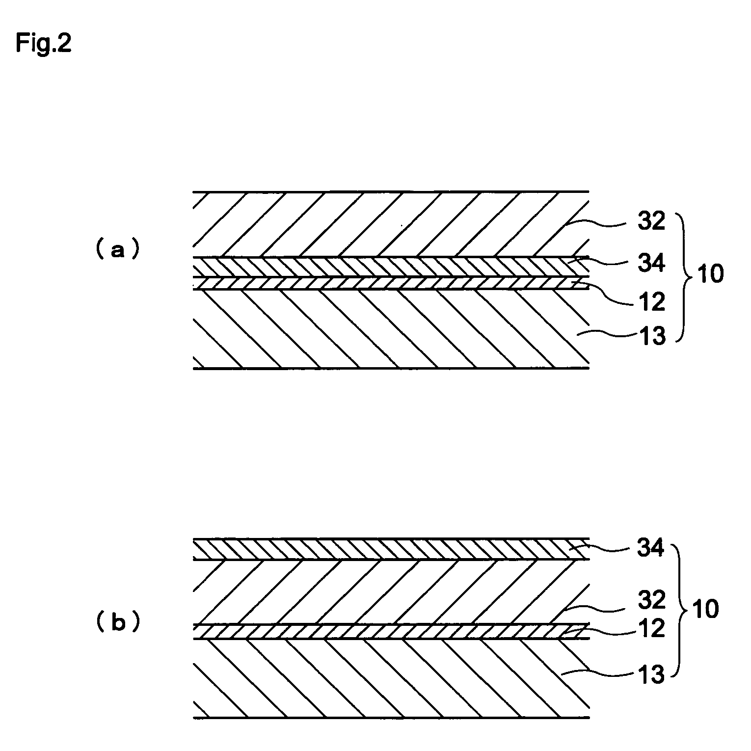
[0060] A first embodiment according to the present invention is directed to, as exemplified in FIG. 1(a) and FIG. 1(b), a single-layer type electrophotographic photoconductor 10 which includes a support base body 13, an intermediate layer 12 and a photoconductor layer 11. Alternatively, as shown in FIG. 2(a) and (b) as examples, the first embodiment of the present invention may be a multi-layer type electrophotographic photoconductor 10 which includes a support base body 13, an intermediate layer 12, a charge generating layer 34 and a charge transferring layer 32. Here, the present invention provides the electrophotographic photoconductor in which the intermediate layer 12 in these electrophotographic photoconductors contains titanium oxide and a binding resin, wherein a ΔL value of the intermediate layer satisfies a following relationship formula (1) or a ΔA value of the intermediate layer satisfies a following relationship formula (2). The electrophotographic pho...

second embodiment

[Second Embodiment]

[0175] A second embodiment of the present invention provides a manufacturing method of an electrophotographic photoconductor which includes a support base body, an intermediate layer and a photoconductor layer, wherein the manufacturing method of the electrophotographic photoconductor includes a step for manufacturing a coating solution for forming the intermediate layer by dispersing titanium oxide in a binding resin solution containing a binding resin and an organic solvent, and a step for forming the intermediate layer in which a ΔL value of the intermediate layer satisfies a following relationship formula (1) or a ΔA value of the intermediate layer satisfies a following relationship formula (2) by using the coating solution for forming a intermediate layer for forming the intermediate layer.

−5.0≦ΔL≦0  (1)

ΔA≦0.055  (2)

[0176]ΔL value: a value which is obtained by subtracting an L value (a parameter value which is measured by a color-difference meter in accordanc...

example 1

1. Formation of Multi-layer Type Electrophotographic Photoconductor

(1) Formation of Intermediate Layer

[0217] In example 1, the obtained coating solution A for forming a intermediate layer is filtered using a 5 micron filter and, thereafter, an aluminum base body (support base body) having a diameter of 30 mm and a length of 238.5 mm is dipped in the obtained coating solution for forming a intermediate layer at a speed of 5 mm / sec with one end thereof directed upwardly thus coating the base body with the coating solution for forming a intermediate layer. Thereafter, curing treatment is applied on the support base body at a temperature of 130° C. for 30 minutes thus forming an intermediate layer having a film thickness of 2 μm.

(2) Formation of Photoconductor Layer

[0218] Next, 1 part by weight of tithanylphthalocyanine which is manufactured in following steps and constitutes a charge generating agent, 1 part by weight of polyvinyl acetal resin (S-LEC KS-5 made by Sekisui Chemica...


PUM


Abstract

The present invention provides an electrophotographic photoconductor which can reduce the generation of fogging under a high-temperature and high-moisture condition and can be easily manufactured, and a method of manufacturing such an electrophotographic photoconductor. In an electrophotographic photoconductor which includes a support base body, an intermediate layer and a photoconductor layer and a manufacturing method of such an electrophotographic photoconductor, the intermediate layer contains titanium oxide and a binding resin and a ΔL value of the intermediate layer satisfies a following relationship formula (1) or a ΔA value of the intermediate layer satisfies a following relationship formula (2), that is, −5.0≦ΔL≦0 (1) and ΔA≦0.055 (2), wherein the ΔL value is a value which is obtained by subtracting an L value (a parameter value which is measured by a color-difference meter in accordance with JIS Z 8722) which is measured with respect to a single support base body from the L value which is measured in a state that the intermediate layer is formed on the support base body, and the ΔA value is a value which is obtained by subtracting reflection absorbance (a parameter value which is measured by a color-difference meter) which is measured with respect to a single support base body from the reflection absorbance which is measured in a state that the intermediate layer is formed on the support base body.

Description

BACKGROUND OF THE INVENTION [0001] 1. Field of the Invention [0002] The present invention relates to an electrophotographic photoconductor and a manufacturing method of an electrophotographic photoconductor. The present invention relates more particularly to a high-quality electrophotographic photoconductor which is used in an image forming apparatus such as a printer, a copying machine, a facsimile or the like and a manufacturing method of such an electrophotographic photoconductor. [0003] 2. Related Art [0004] In an electrophotographic photoconductor provided to an image forming apparatus, a so-called organic photoconductor which is constituted of a charge generating agent which generates charges upon radiation of light, a charge transferring agent which transfers the generated charges, a binding resin which constitutes a layer in which these materials are dispersed or the like has been popularly used. However, the organic photoconductor has following drawbacks. [0005] (1) Along w...

Claims


Application Information

Patent Timeline
Patent Type & Authority Applications(United States)
IPC IPC(8): G03G5/14
CPCG03G5/047G03G5/142G03G5/144
Inventor OTSUBO, JUNICHIROAZUMA, JUNMARUO, KEIJIINAGAKI, YOSHIONAKAI, NORIOHAMASAKI, KAZUNARIOKAWA, SHIHO
Owner KYOCERA DOCUMENT SOLUTIONS INC
Why Eureka
Try Eureka