Method of restoring low-k material or porous low-k layer

a low-k material and low-k layer technology, applied in the field of low-k material processing, to achieve the effect of lowering the k-value of low-k material

Inactive Publication Date: 2007-04-05
UNITED MICROELECTRONICS CORP
View PDF5 Cites 19 Cited by
  • Summary
  • Abstract
  • Description
  • Claims
  • Application Information

AI Technical Summary

Benefits of technology

[0007] In view of the foregoing, this invention provides a method of restoring a low-k material

Problems solved by technology

However, a porous low-k material easily adsorbs moisture, gas or other contaminant during an etching, ashing, washing or chem

Method used


Image

  • Method of restoring low-k material or porous low-k layer
  • Method of restoring low-k material or porous low-k layer
  • Method of restoring low-k material or porous low-k layer

Examples


Embodiment Construction

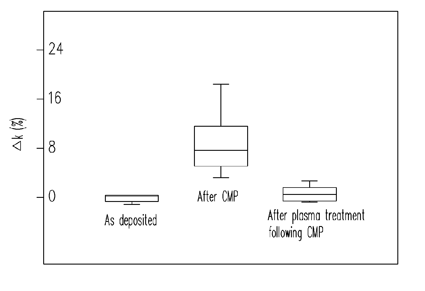
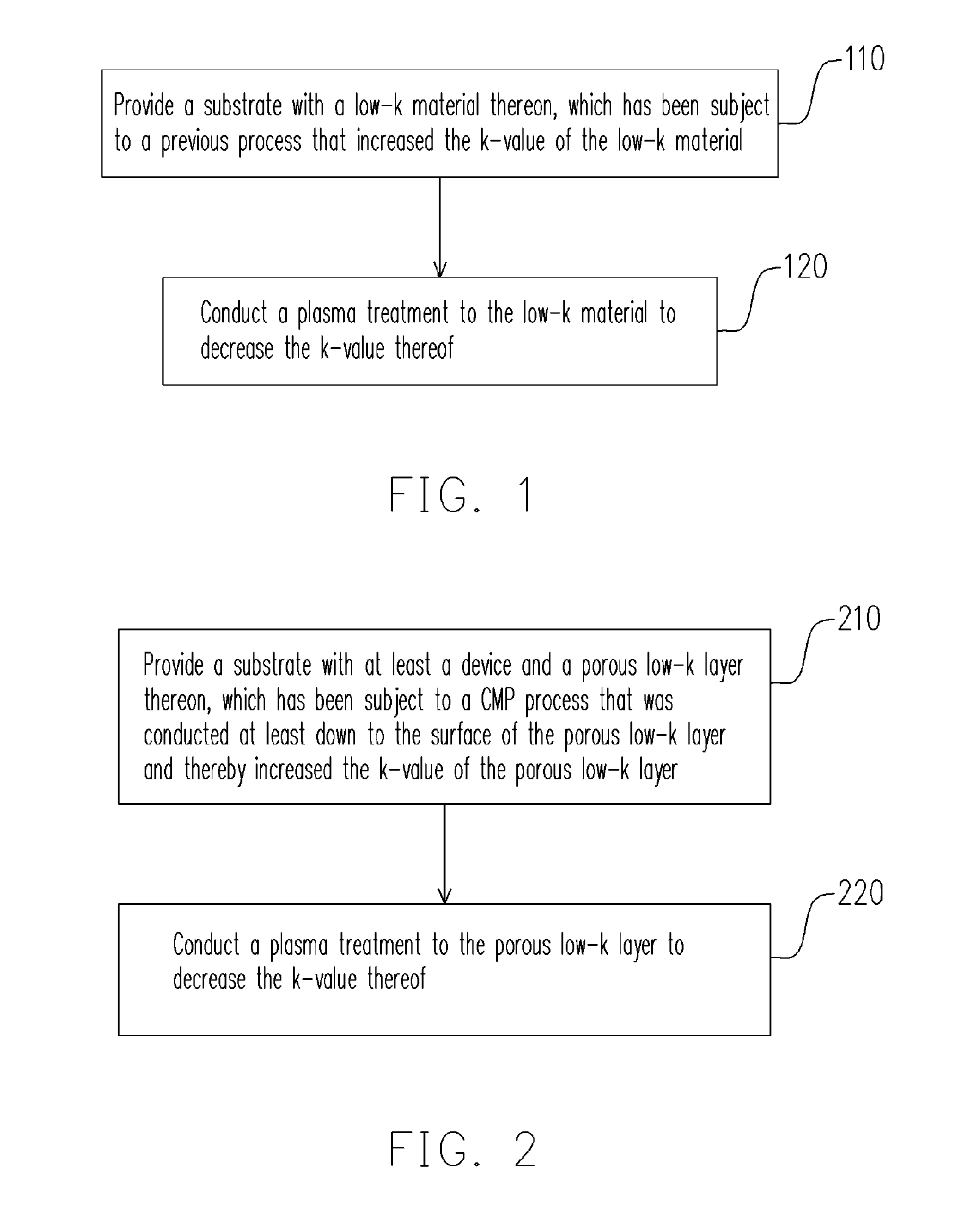
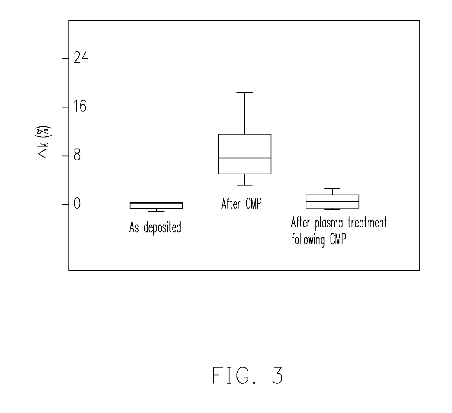
[0019]FIG. 1 is a flow chart of a method of restoring a low-k material according to an embodiment of this invention. In step 110, a substrate with a low-k material thereon is provided, which has been subject to a previous process that raised the k-value of the low-k material. The substrate may have a device therein, such as a MOS transistor or a memory device, and the low-k material may constitute an IMD layer covering a device. The low-k material can be a porous low-k material possibly having a k-value of about 1.0-2.7, such as, carbon-doped oxide (CDO) containing a porogen like a hydrocarbon compound (CxHy), fluorinated amorphous carbon, Parylene AF4, PAE or Cyclotene, etc. The low-k material may be formed through spin-coating, PECVD or high-density plasma (HDP) CVD. The previous process is possibly an etching, washing, ashing or CMP process that raised the k-value of the low-k material by more than 10%.

[0020] In next step 120, a plasma treatment is conducted to the low-k materia...


PUM


Abstract

A method of restoring a low-k material is described, applied to a substrate with a low-k material thereon, wherein the substrate has been subject to a previous process that raised the k-value of the low-k material. The method includes performing a plasma treatment to the low-k material to decrease the k-value thereof.

Description

BACKGROUND OF THE INVENTION [0001] 1. Field of the Invention [0002] The present invention relates to a method of processing a low-dielectric-constant (low-k) material. More particularly, the present invention relates to a method of restoring the dielectric constant (k-value) of a low-k material. [0003] 2. Description of the Related Art [0004] In the rapid development of ultra-large scale integrated circuits, low-k material has become a very important factor in reducing the RC delay effect of the interconnect structure to increase the operation speed. [0005] To make the k-value of a dielectric layer closer to that of air, many porous low-k materials with nanopores or sub-nanometer pores therein have been studied. However, a porous low-k material easily adsorbs moisture, gas or other contaminant during an etching, ashing, washing or chemical mechanical polishing (CMP) process, so that the k-value thereof is raised degrading the original low-k property thereof. [0006] For example, in a...

Claims


Application Information

Patent Timeline
IPC IPC(8): H01L21/4763
CPCH01L21/02107H01L21/02203H01L21/0234H01L21/3105H01L21/31058H01L21/31695H01L21/76826
Inventor CHEN, MEI-LINGCHEN, JEI-MINGLAI, KUO-CHIHSU, WEN-CHIEH
Owner UNITED MICROELECTRONICS CORP
Why Eureka
Try Eureka