Metal capacitor and method of making the same

a metal capacitor and capacitor technology, applied in capacitors, semiconductor devices, semiconductor/solid-state device details, etc., can solve the problems of increasing the surface area of the mom capacitor electrode, the size of the mom capacitor has to be scaled down, and the capacitance of the mom capacitor cannot be provided. , to prevent the rc delay raised, the effect of improving the capacitance of the metal capacitor

Active Publication Date: 2012-02-14
MARLIN SEMICON LTD
View PDF8 Cites 331 Cited by
  • Summary
  • Abstract
  • Description
  • Claims
  • Application Information

AI Technical Summary

Benefits of technology

[0013]The present invention features the use of treatments such as UV radiation, a plasma treatment or an ion implantation to increase the dielectric constant of the dielectric layer in the second region, while the dielectric constant of the dielectric layer in the first region remains the same. In this way, the dielectric layer in the first region maintains a low dielectric constant to prevent RC delay raised between the metal interconnection. The dielectric constant of the dielectric layer in the second region is increased to improve the capacitance of the metal capacitor.

Problems solved by technology

As the complexity and integration of integrated circuits continues to increase, the size of semiconductor elements becomes smaller and smaller.
However, because modern electronic devices are built at the nano scale, the size of the MOM capacitor has to be scaled down.
Under this condition, increasing the surface area of the MOM capacitor electrode can no longer provide enough capacitance.
This, however, results in the capacitance of the MOM capacitor being compromised.
Therefore, the reduced surface area of the capacitor electrode and the low dielectric constant of the capacitor dielectric layer deteriorate the capacitance of the MOM capacitor.

Method used


Image

  • Metal capacitor and method of making the same
  • Metal capacitor and method of making the same
  • Metal capacitor and method of making the same

Examples


Embodiment Construction

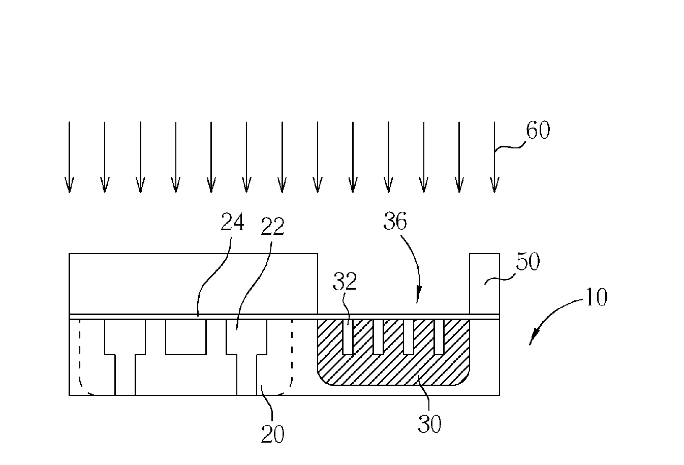
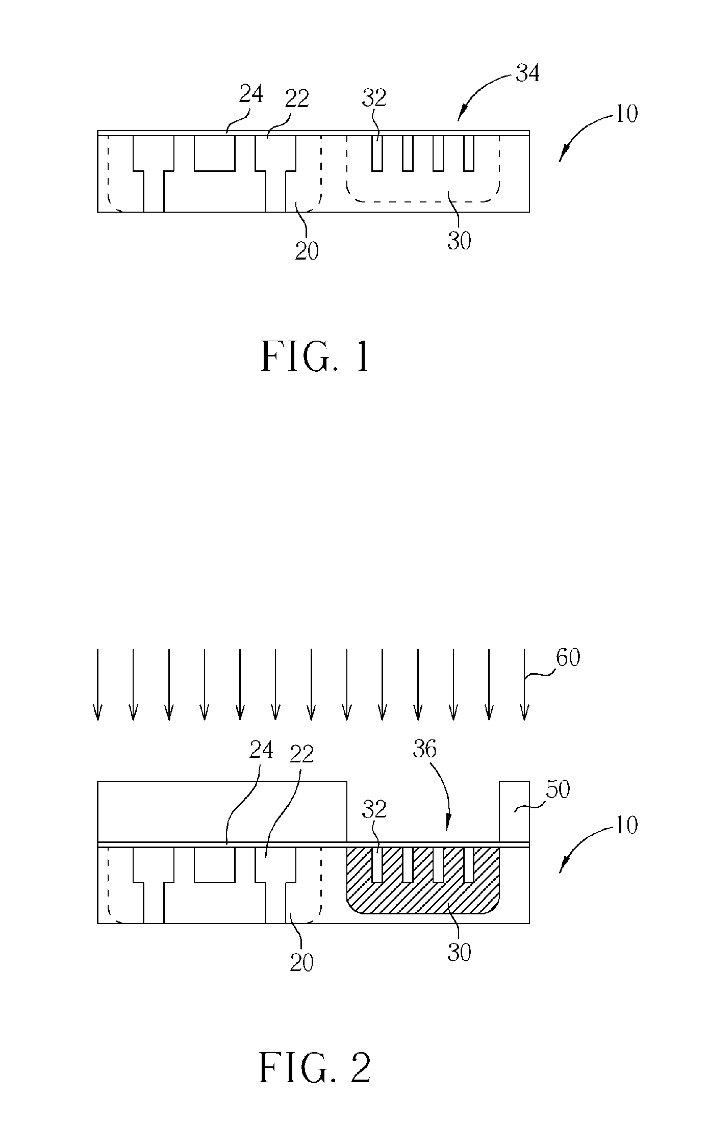
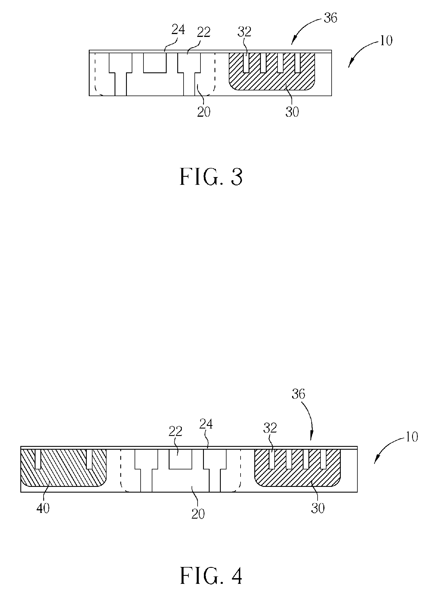
[0017]FIG. 1 to FIG. 4 are schematic diagrams depicting a method of fabricating a metal capacitor. As shown in FIG. 1, a dielectric layer 10 is provided. A first region 20 and a second region 30 are positioned on the dielectric layer 10.

[0018]The dielectric layer 10 can be formed on a semiconductor substrate (not shown) such as a silicon wafer, a silicon on insulator (SOI), a silicon on sapphire (SOS), a silicon on zirconia (SOZ), a doped or undoped semiconductor, a silicon epitaxial layer supported by a semiconductor substrate, or the like. The semiconductor is not limited to silicon, but also can be silicon-germanium, germanium, or germanium arsenide. The dielectric layer 10 is a material that has a low dielectric constant, such as FLARE™, SiLK™, poly(arylene ether) polymer, parylene compounds, polyimide, fluorinated polyimide, hydrogen silsesquioxane (HSQ), methylsilsesquioxane (MSQ), fluorinated silicon glass (FSG),silicon dioxide, nanoporous silica or teflon.

[0019]By performing...


PUM

PropertyMeasurementUnit
dielectric constantaaaaaaaaaa

Abstract

A method of making a metal capacitor includes the following steps. A dielectric layer having a metal interconnection and a capacitor electrode is provided. Then, a treatment is performed to increase the dielectric constant of the dielectric layer surrounding the capacitor electrode. The treatment can be UV radiation, a plasma treatment or an ion implantation. Accordingly, the metal capacitor will have a higher capacitance and RC delay between the metal interconnection and the dielectric layer can be prevented.

Description

BACKGROUND OF THE INVENTION[0001]1. Field of the Invention[0002]The present invention is related to a metal capacitor and a method of making the same, and more particularly, to a structure and a method of improving the capacitance of a metal-oxide-metal (MOM) capacitor.[0003]2. Description of the Prior Art[0004]As the complexity and integration of integrated circuits continues to increase, the size of semiconductor elements becomes smaller and smaller. This has led to a reduction in the overall size of capacitors with the result that the corresponding capacitance is also reduced. Generally, there are three effective ways to improve the capacitance through circuit design. The first way is to decrease the separation between the capacitor electrodes. The second way is to increase the surface area of each capacitor electrode. The third way is to use a dielectric material with a high dielectric constant in the capacitor dielectric layer.[0005]Commonly used capacitors include the metal-in...

Claims


Application Information

Patent Timeline
Patent Type & Authority Patents(United States)
IPC IPC(8): H01L21/8242
CPCH01L21/3105H01L21/76825H01L21/76826H01L23/5223H01L28/40H01L21/312H01L21/3122H01L21/3124H01L21/31612H01L21/31629H01L21/31695H01L2924/0002H01L2924/00
Inventor YANG, CHIN-SHENG
Owner MARLIN SEMICON LTD
Why Eureka
Try Eureka