Apparatus comprising an avalanche photodiode

Active Publication Date: 2007-04-19
LG INNOTEK CO LTD
View PDF11 Cites 14 Cited by
  • Summary
  • Abstract
  • Description
  • Claims
  • Application Information

AI Technical Summary

Benefits of technology

[0018] An aspect of the present invention is the inventors'recognition that the dark count rate is a function of the number of defects located in the device region of an APD, and that the dark count rate can be decreased by reducing the volume of the dev

Problems solved by technology

The curvature of the junction profile in the edge region, however, leads to a larger local electric field and therefore higher gain and lower breakdown voltage than in the active region.
Unfortunately, dark count rate also increases wit

Method used


Image

  • Apparatus comprising an avalanche photodiode
  • Apparatus comprising an avalanche photodiode
  • Apparatus comprising an avalanche photodiode

Examples


Embodiment Construction

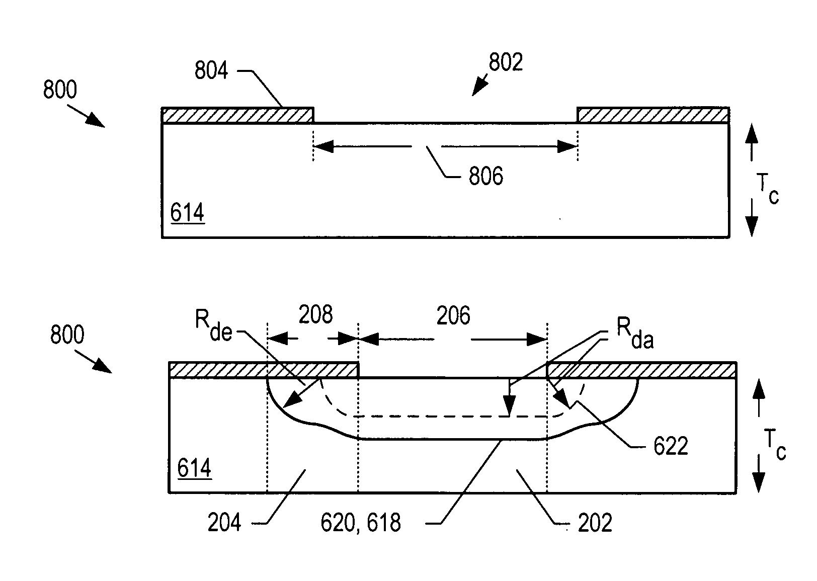
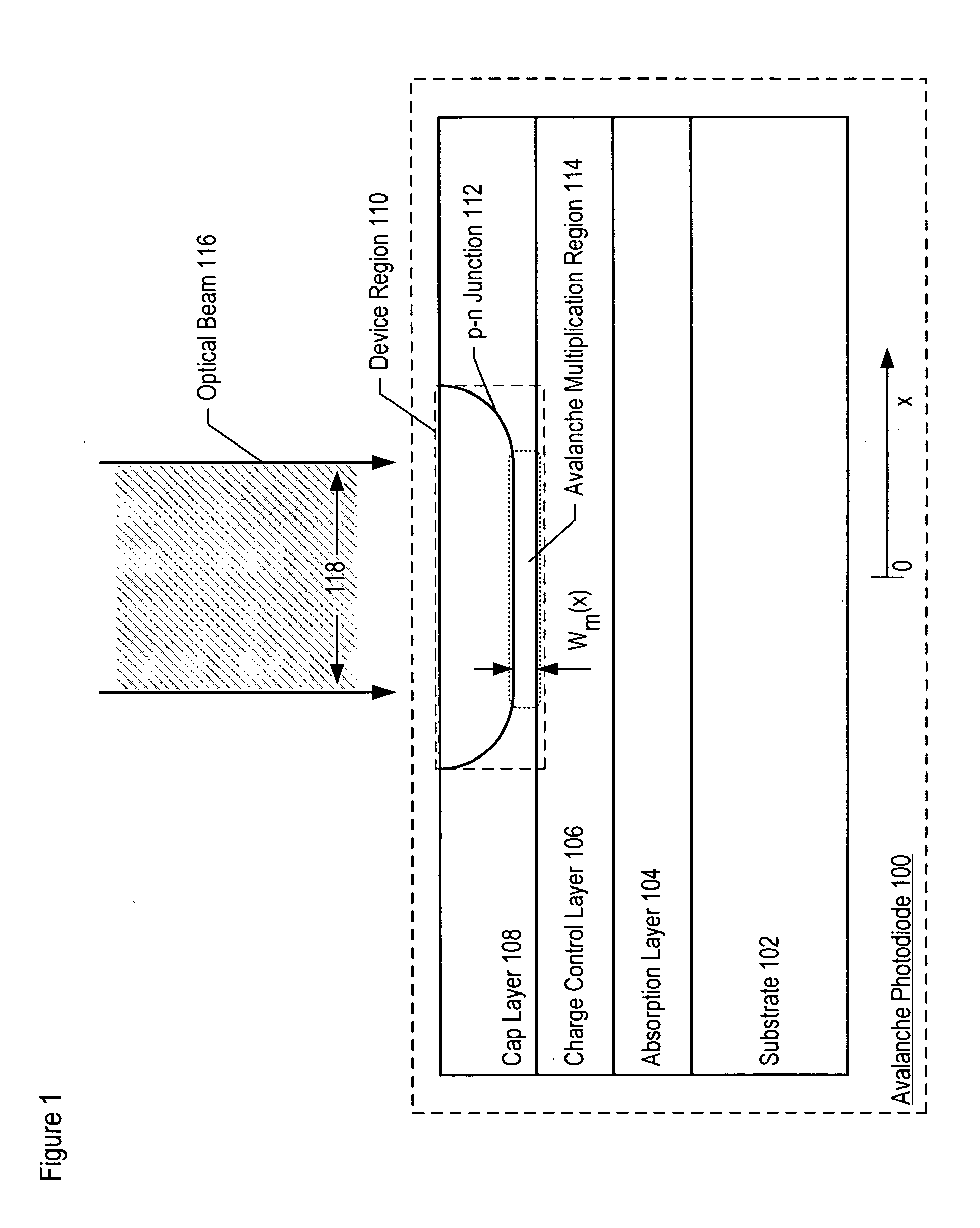
[0034] The following terms are defined for use in this Specification, including the appended claims: [0035] Device region is the portion of the cap layer defined by the lateral extent of the doped portion of the cap layer. The device region includes the full thickness of the cap layer, and therefore includes the undoped portion of the cap layer that resides under the doped portion. For example, the device region includes both the active region and the edge region, as defined below. [0036] Active region means that portion of the cap layer wherein the p-n junction has a substantially uniform doping profile and junction depth (i.e., wherein the p-n junction is a planar junction). The active region extends though the entire thickness of the cap layer, and therefore also includes the avalanche multiplication region under the planar junction. [0037] Edge region means that portion of the cap layer wherein the p-n junction does not have a substantially uniform doping profile and junction de...


PUM


Abstract

Avalanche photodiodes are provided, wherein the APDs provide both high optical coupling efficiency and low dark count rate. The APDs are formed such that their cap layer has an active region of sufficient width to enable high optical coupling efficiency but the APD still exhibits a low dark count rate. These cap layers have a device area with an active region and an edge region, wherein the size of the active region is substantially matched to the mode-field diameter of an optical beam, and wherein the size of the edge region is made small so as to reduce the number of defects included. These APD designs maintain a substantially uniform gain and breakdown voltage, as necessary for practical use.

Description

STATEMENT OF RELATED CASES [0001] This application is related to U.S. Patent Application Attorney Docket No. 293-003US, filed on even date herewith, and incorporated by reference herein. FIELD OF THE INVENTION [0002] The present invention relates to avalanche photodiodes in general and, more particularly, to avalanche photodiodes for use in single-photon detection applications. BACKGROUND OF THE INVENTION [0003] Avalanche photodiode (APD) structures that have separate absorption and multiplication layers (SAM-APDs) can provide electrical output signals with high fidelity (i.e., low noise). In a SAM-APD, the optical energy is absorbed and converted into electrical carriers in a layer specifically designed for efficient absorption (hereinafter, referred to as the “absorption layer”). The resulting electrical signal is amplified in a different layer specifically designed for efficient electrical carrier multiplication (hereinafter, referred to as the “cap layer”). By separating the abs...

Claims


Application Information

Patent Timeline
IPC IPC(8): H01L31/107
CPCH01L31/1075
Inventor ITZLER, MARK ALLENBEN-MICHAEL, RAFAEL
Owner LG INNOTEK CO LTD
Why Eureka
Try Eureka