Semiconductor device

Active Publication Date: 2007-04-19
MICRON TECH INC
View PDF4 Cites 5 Cited by
  • Summary
  • Abstract
  • Description
  • Claims
  • Application Information

AI Technical Summary

Benefits of technology

[0006] It is therefore an object of this invention to provide a semiconductor device which h

Problems solved by technology

As a result, the related semiconductor device has problems that the connecting wires connected to the DQ system pins of the

Method used


Image

  • Semiconductor device
  • Semiconductor device
  • Semiconductor device

Examples


first embodiment

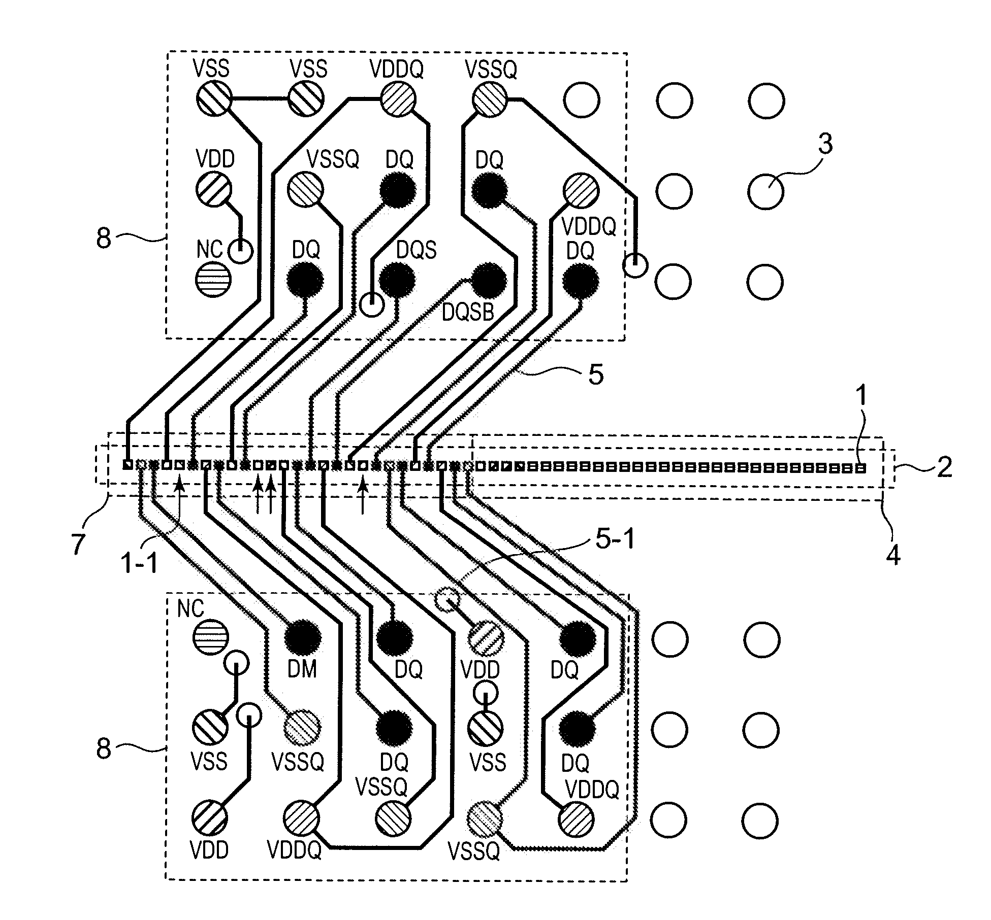
[0042] Referring to FIGS. 7 to 9, a description will be made of a semiconductor device according to this invention.

[0043] The semiconductor device has a semiconductor chip and a package for packaging the semiconductor chip. The semiconductor chip has a pad area along its center line on a surface thereof. A plurality of pads is formed at the pad area (see FIG. 1). The package has pins (or solder balls) (see FIG. 1) which are arranged according to the arrangement standardized by JEDEC (Joint Electron Device Engineering Council) to be mounted on a circuit board. Furthermore, the package has package connecting wires for electrically connecting between these pins and the pads of the semiconductor chip mounted thereon.

[0044] The semiconductor chip has a bonding option or a fuse option to serve as any one of ×4, ×8 and ×16 devices or as one of ×8 and ×16 devices. That is, the semiconductor chip can be used as any one of the ×4, the ×8 and the ×16 devices or one of the ×8 and the ×16 devic...

second embodiment

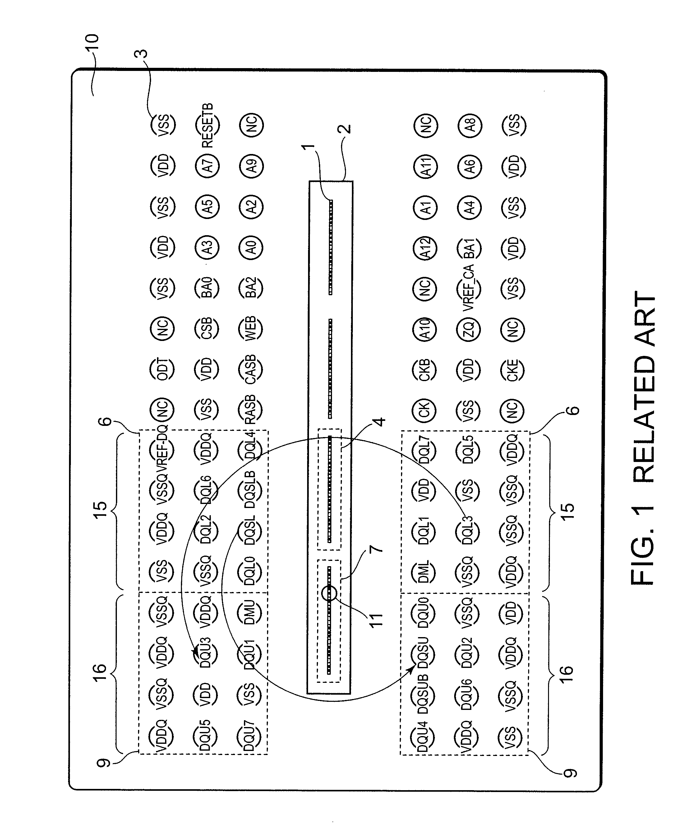
[0065] Referring to FIG. 10, the description will be made about a semiconductor device according to this invention.

[0066] Though FIG. 10, similarly as for FIG. 8, shows the DQ system pad arrangement of the 16-bit structure device, pin arrangement is different from that of FIG. 8. In FIG. 8, the pin arrangement corresponds to ×16 device of DDR3 DRAM standardized by JEDEC and the DQ system high-order bit pin arrangement and the DQ system low-order bit pin arrangement are symmetric with respect to the boundary point. On the other hand, in this embodiment, there is a physical relationship of parallel displacement with respect to the boundary point between the DQ system high-order bit pin arrangement and the DQ system low-order bit pin arrangement. That is, in FIG. 10, if the pin arrangement of the DQ system low-order bit side area is shift toward the left side, it corresponds to the pin arrangement of the DQ system high-order bit side area. Similarly, the pad arrangement of the DQ syste...

third embodiment

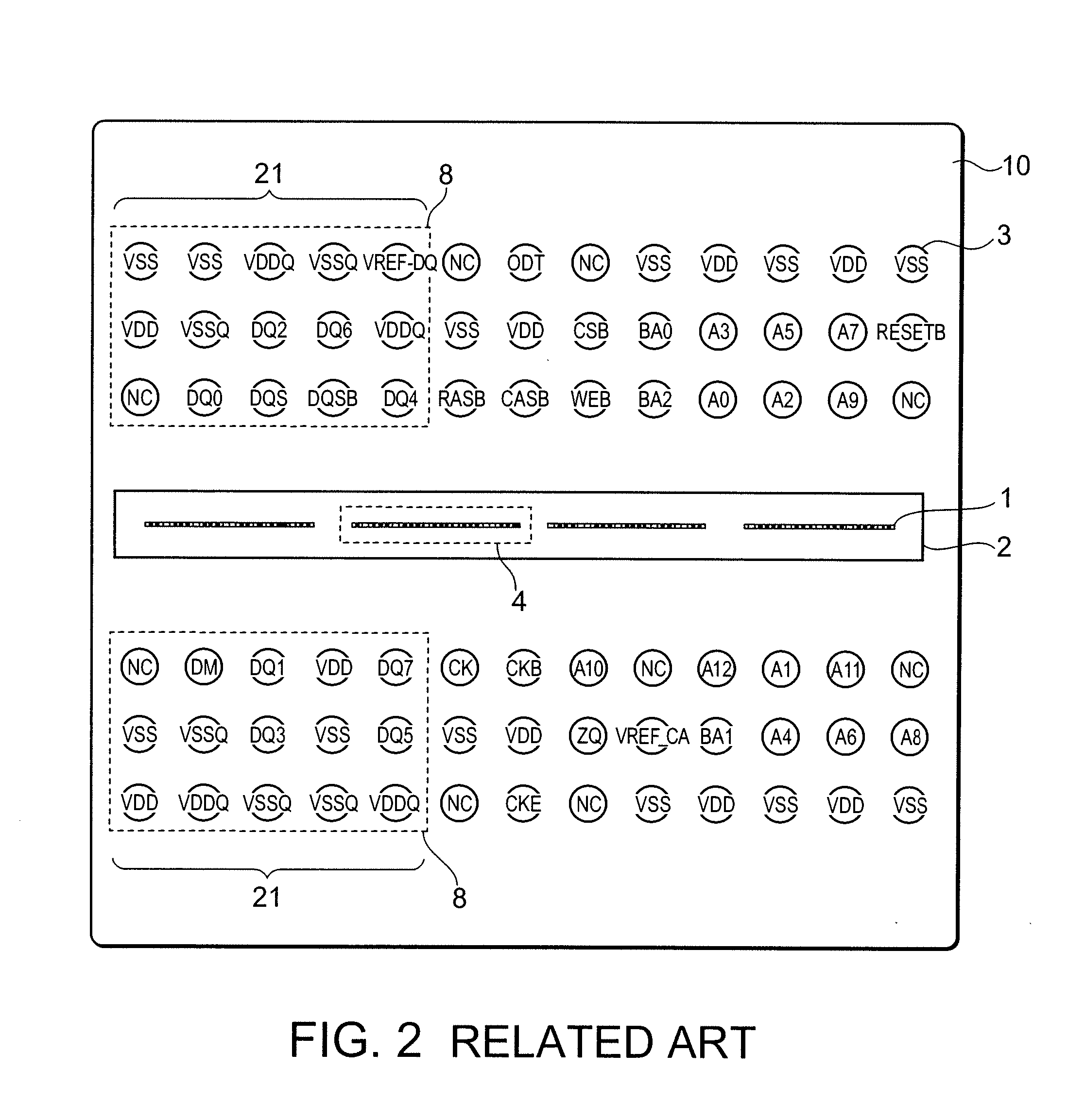
[0069] Referring to FIG. 11, the description will be made about a semiconductor device according to this invention.

[0070]FIG. 11 shows DQ system pad arrangement of a 16-bit structure device, similarly as for FIG. 8. In this embodiment, the DQ system high-order bit side pin arrangement is similar to the pin arrangement that the DQ system low-order bit side pin arrangement is sifted toward left side and reversed with regard to a line of pads. The DQ system high-order bit side pad arrangement is similar to the pad arrangement that the DQ system low-order bit side pad arrangement is sifted toward left side.

[0071] In this embodiment, only two pads are added in comparison with the related semiconductor device, similarly as for the second embodiment. Furthermore, pad assignment change between the ×16 device and the ×4 / ×8l device is made about the same function (i.e. DQ-DQ, DQS-DQS, DM-DM and so on). Accordingly, circuits necessary for the pad assignment change corresponding to the bit str...


PUM


Abstract

A semiconductor device has a semiconductor chip which is usable as any one of 4-bit, 8-bit, and 16-bit structure devices, and a package for packaging the semiconductor chip. The semiconductor chip has first and second DQ pad groups of DQ system pads for said 16-bit structure device. The first DQ pad group is arranged in a first area at a vicinity of a middle part of a surface of the semiconductor chip while the second DQ pad group is arranged in a second area at an outer side of the first area on the surface. An additional pad necessary as one of DQ system pads for the 8-bit structure device except for pads included in the second DQ pad group is formed in the second area.

Description

[0001] This application claims priority to prior application JP 2005-281855, the disclosure of which is incorporated herein by reference. BACKGROUND OF THE INVENTION: [0002] This invention relates to a semiconductor device, in particular, to a semiconductor device that pads connected to package terminals (or pins) are arranged along a center line on a surface of a semiconductor chip. [0003] Recently, improvements in processing or response speed and enlargement of capacity of the semiconductor device are advanced. Moreover, miniaturization of a package is advanced to miniaturize the semiconductor device. A memory device having gigabit memory capacity and mounted on a small sized package has been developed as a dynamic random access memory (hereinafter simply called DRAM). A ball grid array (hereinafter simply called BGA) is known as the small sized package. The BGA having solder balls arranged on a package substrate is a surface mounting type. The BGA is adopted for a general-purpose...

Claims


Application Information

Patent Timeline
IPC IPC(8): H01L23/48
CPCH01L23/49838H01L23/50H01L27/0207H01L27/10897H01L2924/0002H01L2924/00H10B12/50
Inventor ISA, SATOSHIKATAGIRI, MITSUAKICHONAN, TORUNAKAZAWA, SHIGEYUKI
Owner MICRON TECH INC
Why Eureka
Try Eureka