Wiring board, semiconductor device, and method of manufacturing the same

a semiconductor device and wiring board technology, applied in the field of wiring board, semiconductor device and method of manufacturing the same, can solve the problems of poor connection reliability, difficult to make very small wiring connections, and low precision of connection, and achieve high reliability, high yield, and high speed operation

Active Publication Date: 2007-04-12
RENESAS ELECTRONICS CORP
View PDF3 Cites 8 Cited by
  • Summary
  • Abstract
  • Description
  • Claims
  • Application Information

AI Technical Summary

Benefits of technology

[0027] In accordance with the wiring board and semiconductor device of the present invention, a semiconductor device having a short wiring length for connecting to a plurality of semiconductor elements can be provided, and high-speed operation is made possible. Also, since the strength of portions in which stress is concentrated during the manufacturing process is high, high-yield production is made possible without generating wiring breakages and cracks. Reliability is high in the temperature cycles of the semiconductor device itself, and secondary mounting reliability when a semiconductor device is mounted on a printed board is also increased, because the wiring is free from internal stress or very small cracks that cannot be observed from the exterior.

Problems solved by technology

However, in the prior art described above, the connection precision and quality tends to degrade due to the difference in the coefficient of thermal expansion between the substrate and the board of the semiconductor elements.
For this reason, there are problems in that it is difficult to make very small wiring connections to the semiconductor elements, and the connection reliability is poor.
It is therefore difficult to implement a large number of connections between chips having high wiring density by using this prior art.

Method used


Image

  • Wiring board, semiconductor device, and method of manufacturing the same
  • Wiring board, semiconductor device, and method of manufacturing the same
  • Wiring board, semiconductor device, and method of manufacturing the same

Examples


first embodiment

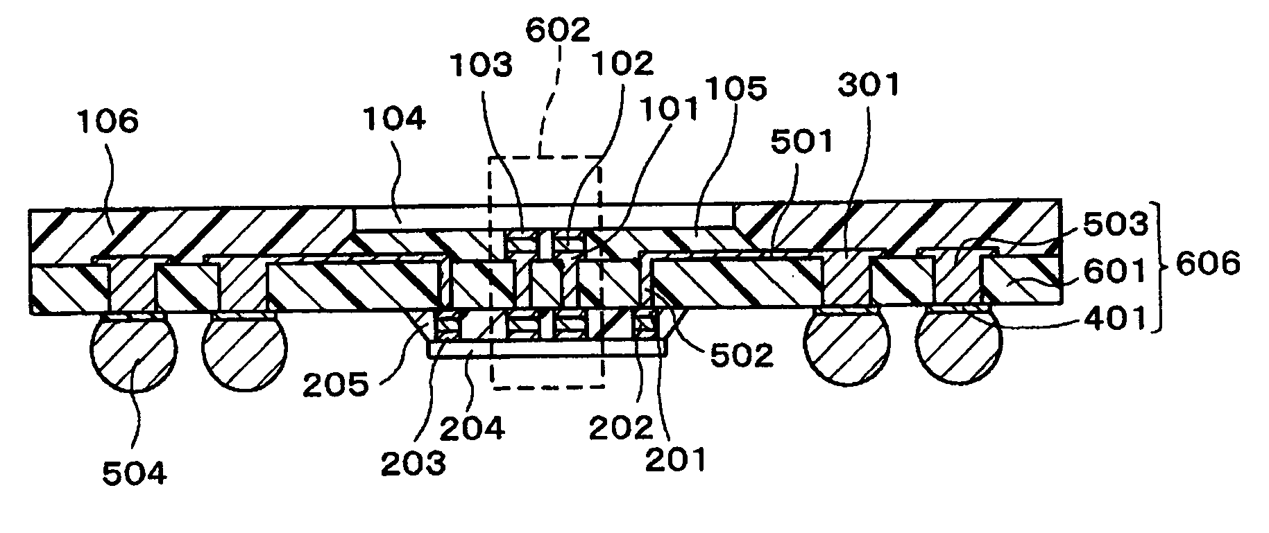
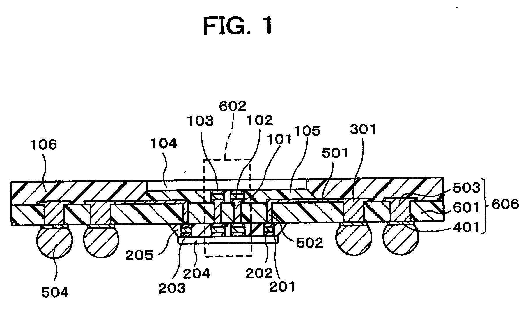
[0040] Embodiments of the present invention are described in detail below with reference to the attached diagrams. Described first is the present invention. FIG. 1 is a diagram that shows the cross-sectional structure of the wiring board 606 of the present embodiment and a semiconductor device 700 that uses the wiring board. BGA balls 504 are connected to the wiring board 606, and the distinctive features are the shape of the BGA lands and the structure for connecting the conductor wiring 501 to the BGA lands 301 to which the BGA balls (not shown in FIG. 1) are connected in specific locations.

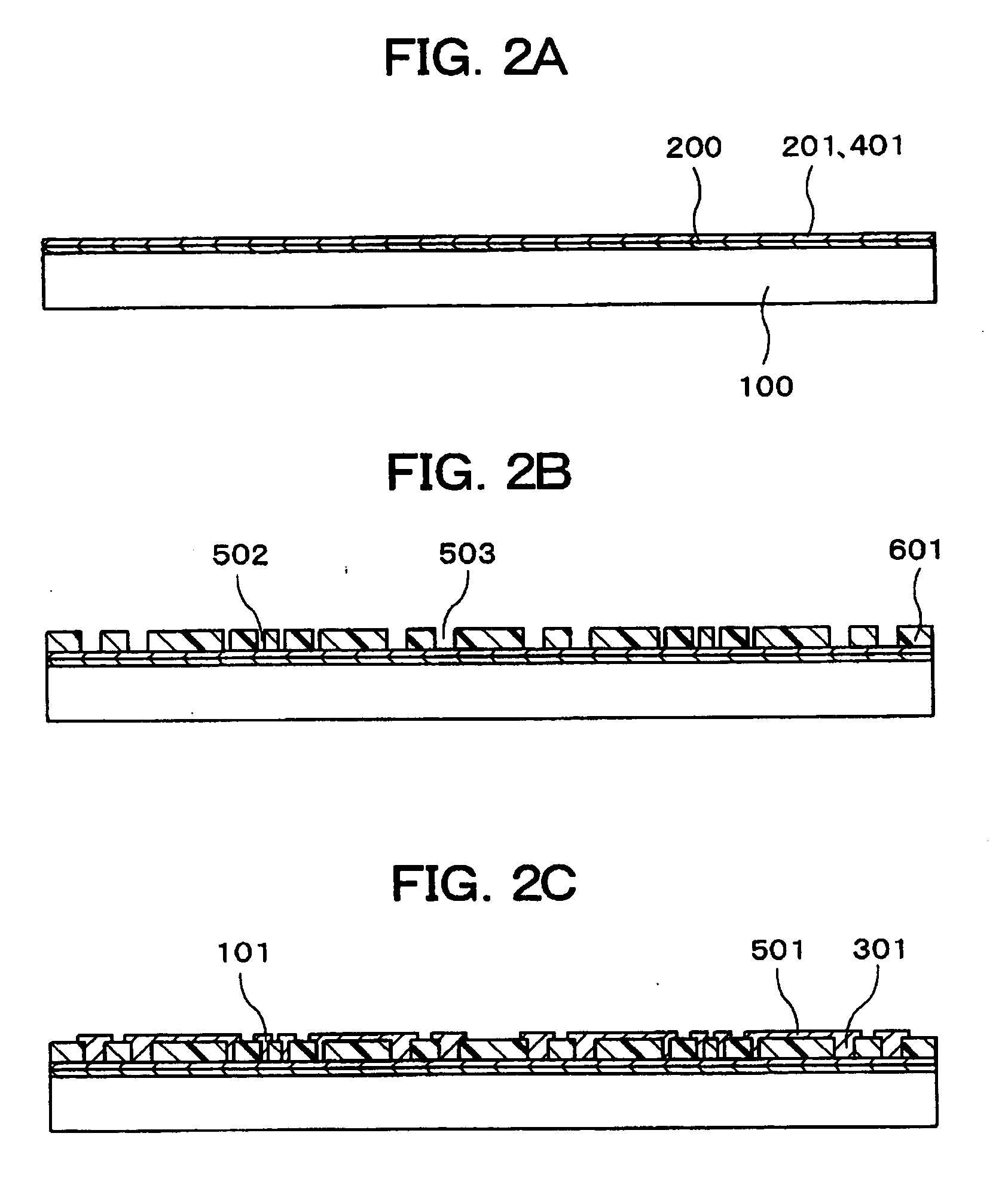
[0041] First, the method of manufacturing the wiring board and semiconductor device of the present embodiment is described with reference to FIGS. 2 to 5. FIGS. 2 to 5 are cross-sectional diagrams showing, as a sequence of steps, the method of manufacturing the wiring board and semiconductor device of the present embodiment. A release layer 200 and a wiring layer ultimately provided with second...

second embodiment

[0051]FIGS. 10A and 10B are enlarged views showing the present invention. The present embodiment features BGA lands in the vicinity of the boundary with the silicon LSI, where peeling is directed from the wiring toward the BGA lands. These lands are shaped so as to gradually increase and then gradually decrease in width in the direction away from the portions connected to the wiring layers formed in the same plane as the lands, and toward one side of the wiring board, as shown in portion C of FIG. 10B.

[0052] The BGA lands and the wiring are radially connected from the center of the semiconductor device toward the external periphery in the same manner as in the prior art. In FIG. 10, the lands are triangularly shaped, and adopting such a shape makes it possible to prevent peeling-induced wiring breakages and cracks from occurring. The cracks and breakages can be prevented because the width of the conductor during peeling does not rapidly increase in contrast to a circular land, even ...


PUM


Abstract

A semiconductor device comprising a flat wiring board, a first LSI disposed on one surface of the wiring board, a sealing resin for covering the one surface and a side face of the first semiconductor element, and a second LSI disposed on another surface of the wiring board. The wiring board has conductive wiring as a wiring layer, an insulation resin as a support layer for the wiring layer, and a conductive through-hole that passes through the wiring layer and the support layer. Connection points between lands disposed in positions in which the external peripheral edges of the semiconductor elements transverse the interior of the lands as viewed vertically from above, which lands are selected from land portions on which the external connection terminals are formed, and the wiring board formed in the same plane as the lands, are unevenly distributed toward one side of the wiring board. Connections for very small wiring are thereby made possible, and a plurality of semiconductor elements can be very densely connected.

Description

BACKGROUND OF THE INVENTION [0001] 1. Field of the Invention [0002] The present invention relates to a wiring board that allows semiconductor devices and the like to be very densely mounted with high precision and that allows a package and module having excellent high-speed and reliability characteristics to be obtained, to a semiconductor device that uses the wiring board, and to a method of manufacturing the same. [0003] 2. Description of the Related Art [0004] The semiconductor device described in Japanese Laid-open Patent Application No. 2001-345418 is an example of a conventional semiconductor device. In this publication, a two-sided mounted structure is disclosed in which semiconductor devices are placed by flip-chip mounting on the two sides of a circuit board. In accordance with the prior art, production yield and reliability can be improved by adjusting the glass transition temperature of the sealing resin that seals the mounted semiconductor devices. [0005] However, in the...

Claims


Application Information

Patent Timeline
Patent Type & Authority Applications(United States)
IPC IPC(8): H05K1/16
CPCH01L21/6835H01L2224/16235H01L23/5383H01L23/5386H01L24/81H01L24/97H01L25/0657H01L2221/68345H01L2224/16H01L2224/81801H01L2224/97H01L2225/06517H01L2225/06572H01L2225/06586H01L2924/01013H01L2924/01029H01L2924/01033H01L2924/01038H01L2924/0104H01L2924/01056H01L2924/01057H01L2924/01073H01L2924/01082H01L2924/09701H01L2924/10329H01L2924/12044H01L2924/14H01L2924/15173H01L2924/15311H01L2924/18161H01L2924/19041H01L2924/19042H01L2924/19043H01L2924/30105H01L23/49816H01L2924/01072H01L2924/01005H01L2924/01006H01L2224/05568H01L2224/05573H01L2924/00014H01L2924/181H01L2924/00H01L2224/05599
Inventor YAMAMICHI, SHINTAROKIKUCHI, KATSUMIKURITA, YOICHIROSOEJIMA, KOJI
Owner RENESAS ELECTRONICS CORP
Why Eureka
Try Eureka