Semiconductor device and method for manufacturing same

Active Publication Date: 2014-11-06
PANASONIC SEMICON SOLUTIONS CO LTD
View PDF11 Cites 2 Cited by
  • Summary
  • Abstract
  • Description
  • Claims
  • Application Information

AI Technical Summary

Benefits of technology

[0038]According to the semiconductor device and a method for manufacturing the semiconductor device in accordance with the present disclosure, high-speed transmission of a signal between the upper and lower chips is enabled by a silicon penetration via-hole in a chip lamination package of chip-on-chip type. Furthermore, an external output

Problems solved by technology

This is because, in two-dimensional miniaturization as in a conventional system on a chip (SoC) structure, data transmission characteristics are degraded by the increase in wiring resistance caused by reduction in th

Method used


Image

  • Semiconductor device and method for manufacturing same
  • Semiconductor device and method for manufacturing same
  • Semiconductor device and method for manufacturing same

Examples


first exemplary embodiment

Semiconductor Device

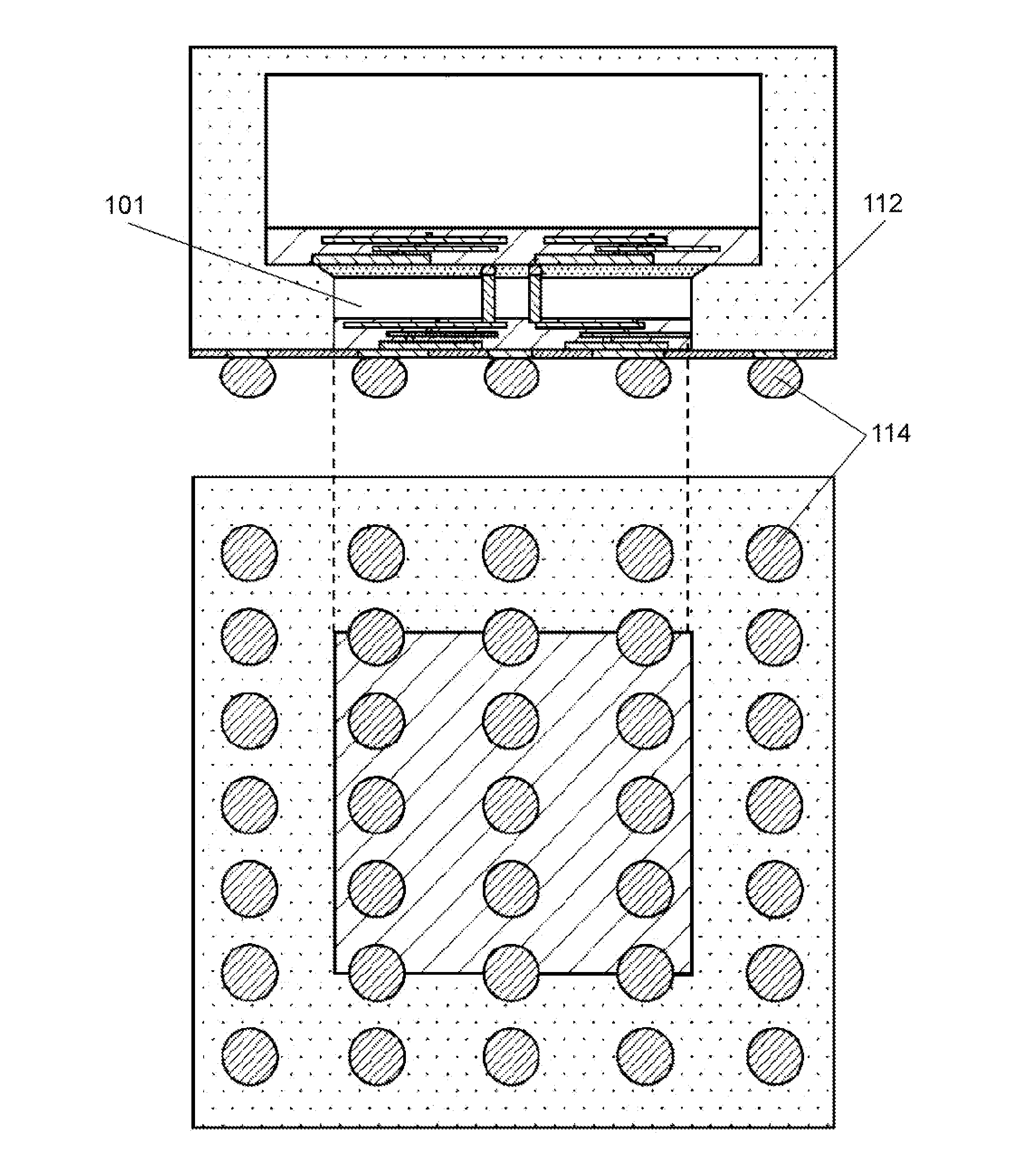
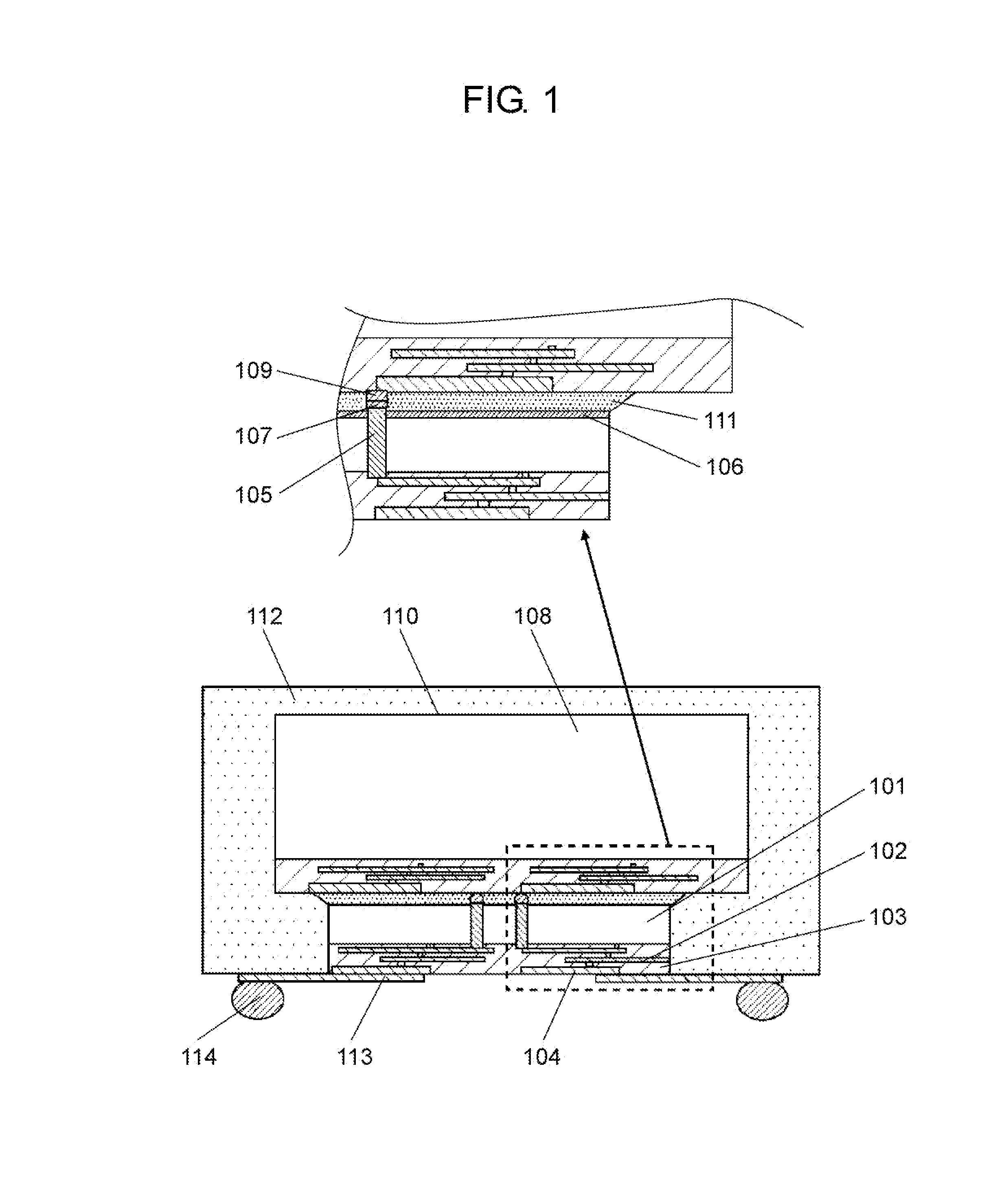
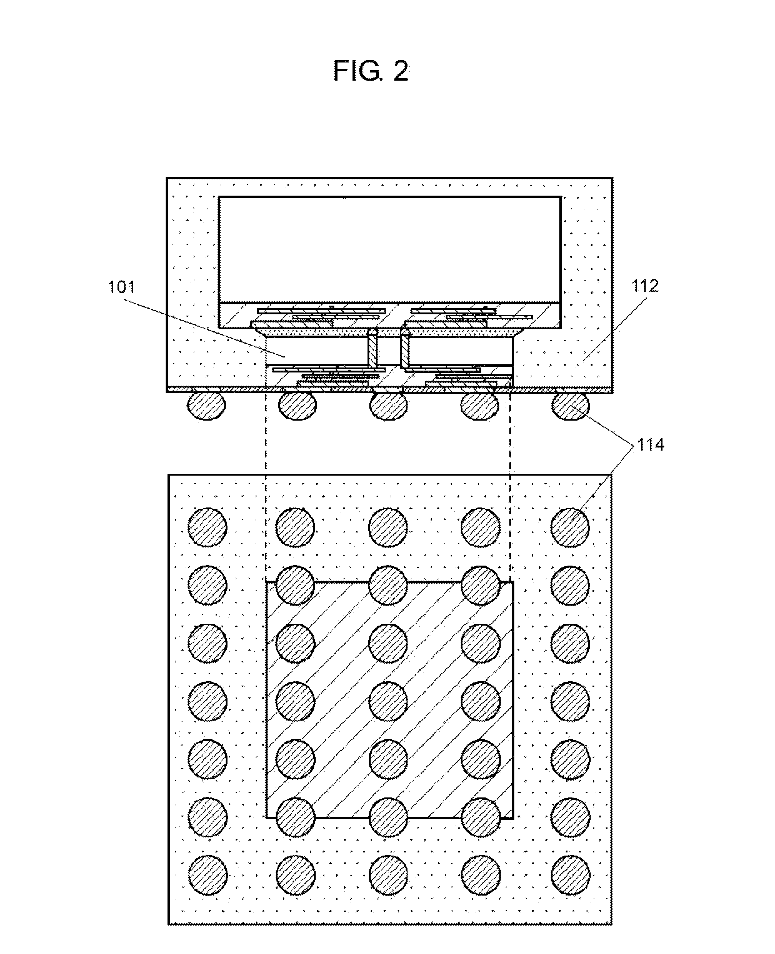
[0065]FIG. 1 is a sectional view showing a semiconductor device in accordance with the first exemplary embodiment.

[0066]As shown in FIG. 1, first semiconductor chip 101 that is made of silicon, for example, and has a main surface of 6 mm□ is prepared. An element (not shown) such as a transistor and distribution layer 104 are formed on the main surface (front surface side) of first semiconductor chip 101. Distribution layer 104 includes wiring 102 electrically connected to the element and inter-layer insulating film 103 covering the element. First semiconductor chip 101 includes silicon penetration electrodes 105 that are connected to a part of wiring 102 and have a diameter of 5 μm and a depth of 50 μm, for example.

[0067]First semiconductor chip 101 is thinned to a thickness of 50 μm or less, for example, by polishing the silicon on the rear surface side. Conductive surfaces of the bottoms of silicon penetration electrodes 105 are exposed on the rear surface of f...

first modified example of first exemplary embodiment

[0086]As shown in FIG. 5, the rear surface and side surfaces of second semiconductor chip 108 may be exposed. This structure can be easily achieved by a process of polishing the rear surface after the sealing, or a process of protecting the rear surface with a sheet before the sealing, and peeling the sheet after the sealing. Also in FIG. 1 to FIG. 4, the rear surface of second semiconductor chip 108 may be exposed.

[0087]In such a structure, heat can be directly radiated to the periphery (in air) through the chip rear surface. Furthermore, a radiator plate, a heat sink, or a fin can be bonded to the chip rear surface, so that a large radiation path can be secured. As a result, a semiconductor device of high radiation property can be provided.

second modified example of first exemplary embodiment

[0088]As shown in FIG. 6, two facing side surfaces of first semiconductor chip 101 may be exposed from first resin 112. In this case, two facing side surfaces other than the exposed two facing side surfaces are covered with first resin 112. In FIG. 6, the rear surface of second semiconductor chip 108 is covered with first resin 112, and side surfaces of second semiconductor chip 108 are exposed. However, the rear surface of second semiconductor chip 108 may be exposed (not shown) as in the first modified example. The side surfaces of second semiconductor chip 108 may be covered with first resin 112 (not shown).


PUM


Abstract

A lamination structure includes a first semiconductor chip and a second semiconductor chip stacked via a bonding section so that a rear surface of the first semiconductor chip faces the main surface of the second semiconductor chip. At least a part of a side surface of the first semiconductor chip are covered with a first resin, a distribution layer is formed on the plane formed of the main surface of the first semiconductor chip and a surface of the first resin. At least part of electrodes existing in the main surface of the second semiconductor chip is electrically connected to at least part of first external electrodes formed on the distribution layer via the penetration electrodes that penetrate the first semiconductor chip.

Description

[0001]This is a continuation of International Application No. PCT / JP2013 / 000071, with an international filing date of Jan. 11, 2012, which claims priority of Japanese Patent Application No. 2012-025777, filed on Feb. 9, 2012, the contents of each of which are hereby incorporated by reference.BACKGROUND[0002]1. Technical Field[0003]The present disclosure relates to a semiconductor device and a method for manufacturing the semiconductor device, specifically to a semiconductor device including a chip-chip lamination or a chip-wafer lamination.[0004]2. Description of the Related Art[0005]Recently, three-dimensional integration by chip lamination has been disclosed in response to improvement in the integration, enhancement in the functionality, and increase in the speed of semiconductor integrated circuit devices (for example, Unexamined Japanese Patent Publication No. 2006-080145, and ITRS 2007 Assembly and Package Chapter, p. 41).[0006]This is because, in two-dimensional miniaturizatio...

Claims


Application Information

Patent Timeline
IPC IPC(8): H01L23/00H01L21/82
CPCH01L24/01H01L21/82H01L24/80H01L2224/04105H01L2224/12105H01L2224/16145H01L2224/32145H01L2224/73204H01L2224/93H01L23/3114H01L21/568H01L24/94H01L25/0657H01L2224/13025H01L2224/94H01L2924/15311H01L2225/06513H01L2225/06541H01L2225/06568H01L2224/14131H01L2224/02379H01L2224/13005H01L23/481H01L24/92H01L24/96H01L24/97H01L2224/05548H01L2224/16238H01L2224/9202H01L2224/96H01L2224/97H01L2224/14135H01L2224/83104H01L2224/0401H01L24/19H01L2224/16225H01L2224/73259H01L2224/92224H01L2924/00012H01L2224/81H01L2924/00014H01L2224/03H01L2224/11H01L2924/206H01L2224/83H01L23/3185H01L2224/02381
Inventor AOI, NOBUOSASAGO, MASARUMORI, YOSHIHIROKAWABATA, TAKESHIYUI, TAKASHIFUJII, TOSHIO
Owner PANASONIC SEMICON SOLUTIONS CO LTD
Why Eureka
Try Eureka