Electron beam exposure apparatus, electron beam exposure apparatus calibration method, and semiconductor element manufacturing method

Active Publication Date: 2005-07-12
CANON KK +2
View PDF0 Cites 7 Cited by
  • Summary
  • Abstract
  • Description
  • Claims
  • Application Information

AI Technical Summary

Benefits of technology

[0012]The control section may adjust the timing of irradiating the electron beam on the wafer by synchronizing timing of deactivating the control signal with timing at which the deflecting section is to stop the deflection of the electron beam.
[0013]The electron beam exposure apparatus may further include a temperature detector for detecting temperature of the control section. The control section may supply the control signal to the load circuit and synchronize the timing of activating the control signal with the timing at which the deflecting section is to deflect the electron beam when a temperature change detected by the temperature detector is more than a predetermined value.
[0014]The control section may supply the control signal to the load circuit and synchronize the timing of activating the control signal with the timing at which the deflecting section is to deflect the electron beam in a predetermined time interval.
[0015]The control section may supply the control signal to the load circuit and synchronize the timing of activating the control signal with the timing at which the deflecting section is to deflect the electron

Problems solved by technology

When the control section calibrates the timing of the control signal and while the deflecting section is connected to the control section, it is difficult to detect the timing of the control signal correctly because a reflected signal reflected from the deflecting section is mixed with the control signal which is to be calibrated.
However, since impedance of the circuit driven by the control signal, wh

Method used


Image

  • Electron beam exposure apparatus, electron beam exposure apparatus calibration method, and semiconductor element manufacturing method
  • Electron beam exposure apparatus, electron beam exposure apparatus calibration method, and semiconductor element manufacturing method
  • Electron beam exposure apparatus, electron beam exposure apparatus calibration method, and semiconductor element manufacturing method

Examples


Embodiment Construction

[0027]The invention will now be described based on the preferred embodiments, which do not intend to limit the scope of the present invention, but exemplify the invention. All of the features and the combinations thereof described in the embodiment are not necessarily essential to the invention.

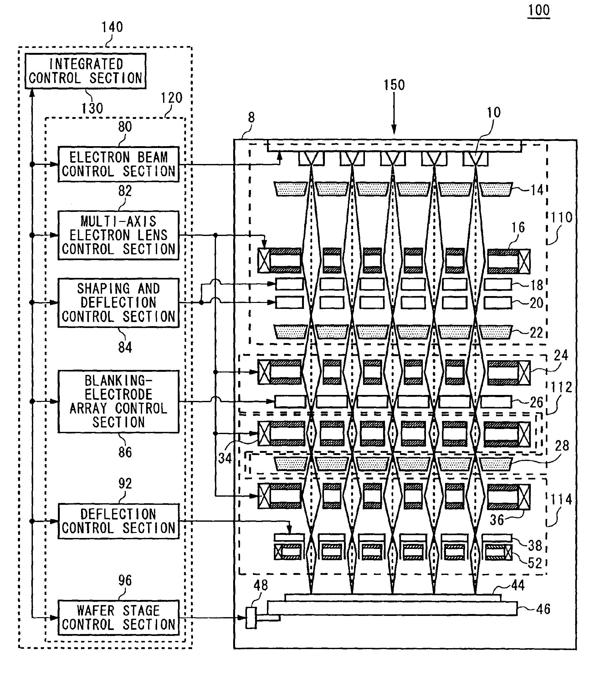
[0028]FIG. 1 is a schematic view showing a configuration of an electron beam exposure apparatus 100 according to an embodiment of the present invention. The electron beam exposure apparatus 100 includes an exposure section 150 for performing a predetermined exposure processing on a wafer 44 by an electron beam, and a control system 140 for controlling an operation of each component of the exposure section 150.

[0029]The exposure section 150 includes an electron optics system, which includes: electron beam shaping means 110 for generating a plurality of electron beams in a chamber 8 and shaping cross-sectional shapes of the electron beams into desired shapes; irradiation status switching means ...


PUM


Abstract

An electron beam exposure apparatus for controlling deflection timing of an electron beam with high precision, including: a blanking-electrode array having a deflecting electrode for deflecting an electron beam; a deflection timing control section for outputting the control signal for controlling the blanking-electrode array; a load circuit, of which the impedance is the same as that of the blanking-electrode array, where the wire length between the deflection timing control section and the load circuit is shorter than the wire length between the deflection timing control section and the deflecting electrode of the blanking-electrode array; and a switching section, connecting with the deflection timing control section, the blanking-electrode array, and the load circuit, for switching the destination of the control signal output from the deflection timing control section between the blanking-electrode array and the load circuit.

Description

BACKGROUND OF THE INVENTION[0001]This patent application claims priority on a Japanese patent application No. 2002-284255 filed on Sep. 27, 2002, the contents of which are incorporated herein by reference.[0002]1. Field of the Invention[0003]The present invention relates to an electron beam exposure apparatus, an electron beam exposure apparatus calibration method, and a semiconductor element manufacturing method. More particularly, the present invention relates to an electron beam exposure apparatus for controlling deflection timing of an electron beam with high precision.[0004]2. Description of Related Art[0005]In an electron beam exposure apparatus for exposing a wafer by an electron beam, it is necessary to control deflection timing of the electron beam with high precision. For that purpose, it is necessary for the control section, which controls the deflecting section, to calibrate timing of control signal for controlling a deflecting section with high precision. When the contr...

Claims


Application Information

Patent Timeline
IPC IPC(8): G03F7/20G21K1/00G21K1/087H01J37/317H01J37/147H01J37/305H01L21/027
CPCB82Y10/00B82Y40/00G21K1/087H01J37/3174H01J37/3177H01J2237/0435H01J2237/30433
Inventor HASHIMOTO, SHIN-ICHIYODA, HARUOMURAKI, MASATO
Owner CANON KK
Why Eureka
Try Eureka