Method and apparatus for switching on a voltage supply of a semiconductor circuit and corresponding semiconductor circuit

a voltage supply and semiconductor technology, applied in the direction of pulse automatic control, pulse manipulation, pulse technique, etc., can solve the problems of uncontrolled switching operation, violation of timing behavior, additional current on the supply line of the semiconductor, etc., to achieve the threshold voltage, the effect of rapid attainmen

Active Publication Date: 2007-04-19
INFINEON TECH AG
View PDF4 Cites 8 Cited by
  • Summary
  • Abstract
  • Description
  • Claims
  • Application Information

AI Technical Summary

Benefits of technology

[0017] Since, as already described hereinbefore, only a low current flows through the transistor until the Miller plateau is reached, it is advantageous to optimize the voltage characteristic between the control input and the first terminal of the transistor in such a way that the threshold voltage of the transistor is attained as quickly as possible.
[0018] In accordance with the disclosure, rapid attainment of the threshold voltage can also be achieved in that a time interval which elapses until a step height, with which the voltage between the control input and the first terminal of the transistor is increased stepwise, is shorter until attainment of the Miller plateau than after attainment of the Miller plateau. In other words, the steps in the time characteristic of the voltage between the control input and the first terminal of the transistor are increased faster and more frequently in time up to the threshold voltage than after attainment of the Miller plateau.

Problems solved by technology

Uncontrolled switching operations (glitches) can occur during the reconnection process and cause additional current on supply lines of the semiconductor circuit in addition to the load current for the capacitors.
This causes a high IR drop (a drop in the supply voltage due to resistive influences), which temporarily reduces the supply voltage of circuit portions adjoining the voltage blocks which have just been switched on and can thus lead to violation of the timing behavior and to disturbances in operation in these circuit portions, also known as soft error.
In addition to the circuit peaks caused by the resistive drop in voltage, the rise rate, at which the load current rises, also leads to problems when the voltage supply is switched on.
also lead to a voltage drop in the supply voltage which is proportional to the rise rate.

Method used


Image

  • Method and apparatus for switching on a voltage supply of a semiconductor circuit and corresponding semiconductor circuit
  • Method and apparatus for switching on a voltage supply of a semiconductor circuit and corresponding semiconductor circuit
  • Method and apparatus for switching on a voltage supply of a semiconductor circuit and corresponding semiconductor circuit

Examples


Embodiment Construction

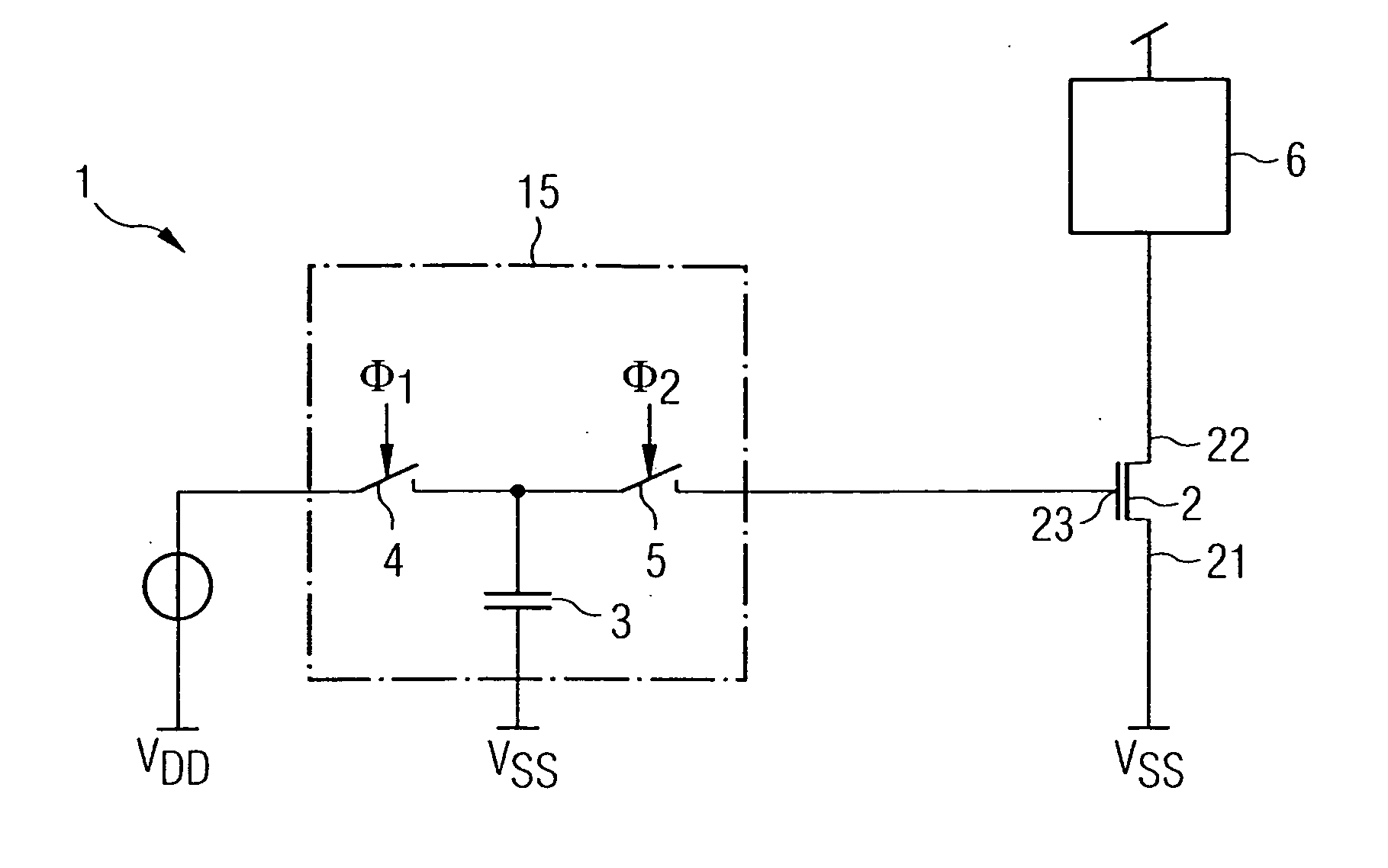
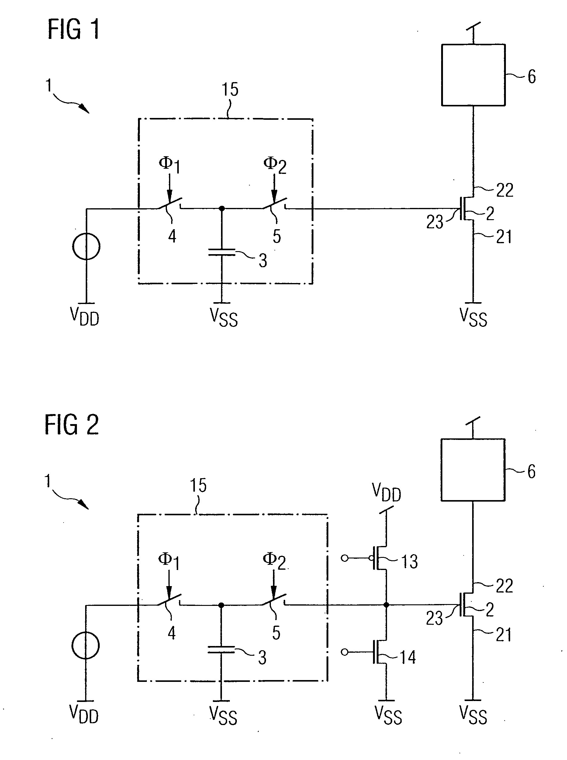
[0044]FIG. 1 shows one embodiment of an apparatus 1 for switching on a voltage supply of a voltage domain 6 of a semiconductor circuit. The voltage domain 6 is connected via a NMOS transistor 2 of the apparatus 1 to VSS of the semiconductor circuit, the source-terminal 21 of the NMOS transistor 2 to VSS, the drain terminal 22 of the NMOS transistor 2 to the voltage domain 6 and the control input or gate terminal 23 of the NMOS transistor 2 being activated by control means 15 of the apparatus 1. The control means 15 comprise a first switch 4, a second switch 5 and a pump capacitor or a capacitor 3 which is connected to VSS via a first terminal. The first switch 4 is connected by its first terminal to VDD while its second terminal is connected to a second terminal of the capacitor 3 and a first terminal of the second switch 5. A second terminal of the second switch 5 is connected to the gate terminal 23. While the first switch 4 is clocked at a first clock rate φ1, the second switch i...


PUM


Abstract

A method and an apparatus for switching on a voltage supply of a voltage domain of a semiconductor circuit is disclosed. A voltage supply is connected to a supply voltage of the semiconductor circuit by means of a switchable element. The switchable element is activated in such a way that, for switching on the voltage supply of the voltage domain, a current through the switchable element rises progressively with at least one intermediate value, in particular stepwise manner.

Description

RELATED APPLICATIONS [0001] The present application claims priority to German Application No DE 10 2005 038 231.2, filed Aug. 12, 2005, the entirety of which is hereby incorporated herein by reference. BACKGROUND OF THE DISCLOSURE [0002] The present disclosure relates to a method and an apparatus for switching on a voltage supply of a semiconductor circuit and to a correspondingly configured semiconductor circuit. [0003] The switching off of unrequired circuit blocks of a semiconductor circuit is a proven method of reducing leakage current losses in intermittently unrequired circuit portions. Once they have been switched off, the inner capacitors of the switched off circuit blocks discharge. These capacitors have to be recharged once they have been switched on again. Uncontrolled switching operations (glitches) can occur during the reconnection process and cause additional current on supply lines of the semiconductor circuit in addition to the load current for the capacitors. Conseq...

Claims


Application Information

Patent Timeline
Patent Type & Authority Applications(United States)
IPC IPC(8): H03L7/00
CPCH03K17/163H03K17/567H03K17/687
Inventor HENZLER, STEPHANBERTHOLD, JORGPACHA, CHRISTIANSCHMITT-LANDSIEDEL, DORISNIRSCHL, THOMASGEORGAKOS, GEORG
Owner INFINEON TECH AG
Why Eureka
Try Eureka