Liquid crystal display apparatus

a technology of liquid crystal display and display screen, which is applied in the direction of instruments, semiconductor devices, optics, etc., can solve the problems of insufficient improvement, high cost and high production cost of highly fine wiring substrates, etc., and achieves the effects of improving emission efficiency, high brightness, and increasing siz

Active Publication Date: 2007-04-19
PANASONIC LIQUID CRYSTAL DISPLAY CO LTD +1
View PDF1 Cites 47 Cited by
  • Summary
  • Abstract
  • Description
  • Claims
  • Application Information

AI Technical Summary

Benefits of technology

[0026] Advantageously, in the present invention, consumptive power in the backlight module representing a light source of LED element structure for use in the liquid crystal display apparatus can be reduced. This advantage is due to the fact that high brightness can be attained by increasing the size without degrading the uniformity of current density distribution in the LED unit element and light can be taken out from the transparent substrate side on account of the flip chip mounting, so that the emission efficiency can be improved nearly twice in comparison to the case of wire bonding mounting. With the current efficiency and power efficiency promoted nearly twice, the consumptive power can be reduced for maintaining the same brightness. In other words, with the efficiency improved, the same brightness can be attained with a smaller number of mounted LED unit elements, thus reducing the number of LED unit elements and consequently reducing the consumptive power to advantage. Even in an element structure subject to wire bonding mounting, the construction of the present invention can be applied to ensure that improvements in efficiency and reduction of consumptive power can be expected as compared to the case of conventional element structure.
[0027] In the phase of mounting, simplified mounting can be allowed and the yield of mounting can be improved to advantage. This is because with the size of element structure increased, the electrode pattern can be swelled and bumps formed on the highly symmetrical electrode pattern can be positioned in good balance to the wiring pattern. In comparison with an element structure of relatively small area, the accuracy of positioning can be improved and the yield of flip chip mounting using thermo crimp or ultrasonic crimp can be promoted.
[0028] Further, as compared to the case where an electrode pattern is newly developed by increasing the size of a light emitting diode element constituting a light source, an element structure of enlarged area having a plurality of electrodes by using unit elements of small area put on market can obviously be reduced in costs to advantage. This is because in the small-size unit element which has already been commercialized, the technique for electrode formation and the electrode pattern are promoted up to the technique meeting products, sufficiently upgrading the yield and reliability, and therefore conditions for processes are settled and the element shape is stable. In the present invention, quite the same process conditions can be applied by merely changing the mask necessary for periodicity of electrode patterns. Thus, the high process yield and mounting yield can be maintained.
[0029] By improving the emission efficiency of the element structure as a whole, the compatibility between low consumptive power and low cost can be assured. Because of materialization of the high process yield and high mounting yield and dispensability of a new element structure, the element structure can be formed at relatively low costs.

Problems solved by technology

In making an attempt to increase the size of the LED element for flip chip mounting with the aim of realizing high brightness in the prior art, the area of electrodes swells and uniform distribution of current density from positive electrode to negative electrode is difficult to achieve, raising a problem that a sufficient improvement cannot be made even when the prior art interdigitated array electrode or lattice electrode as above is applied.
For performing flip chip mounting in a small-sized LED element, a highly fine wiring pattern is necessary and a highly precise mounting technique is needed and therefore, preparation of a highly fine wiring substrate applied with a high-cost process is required.

Method used


Image

  • Liquid crystal display apparatus
  • Liquid crystal display apparatus
  • Liquid crystal display apparatus

Examples


embodiment 1

[0107] A first embodiment of the invention will first be described with reference to FIGS. 1 to 30.

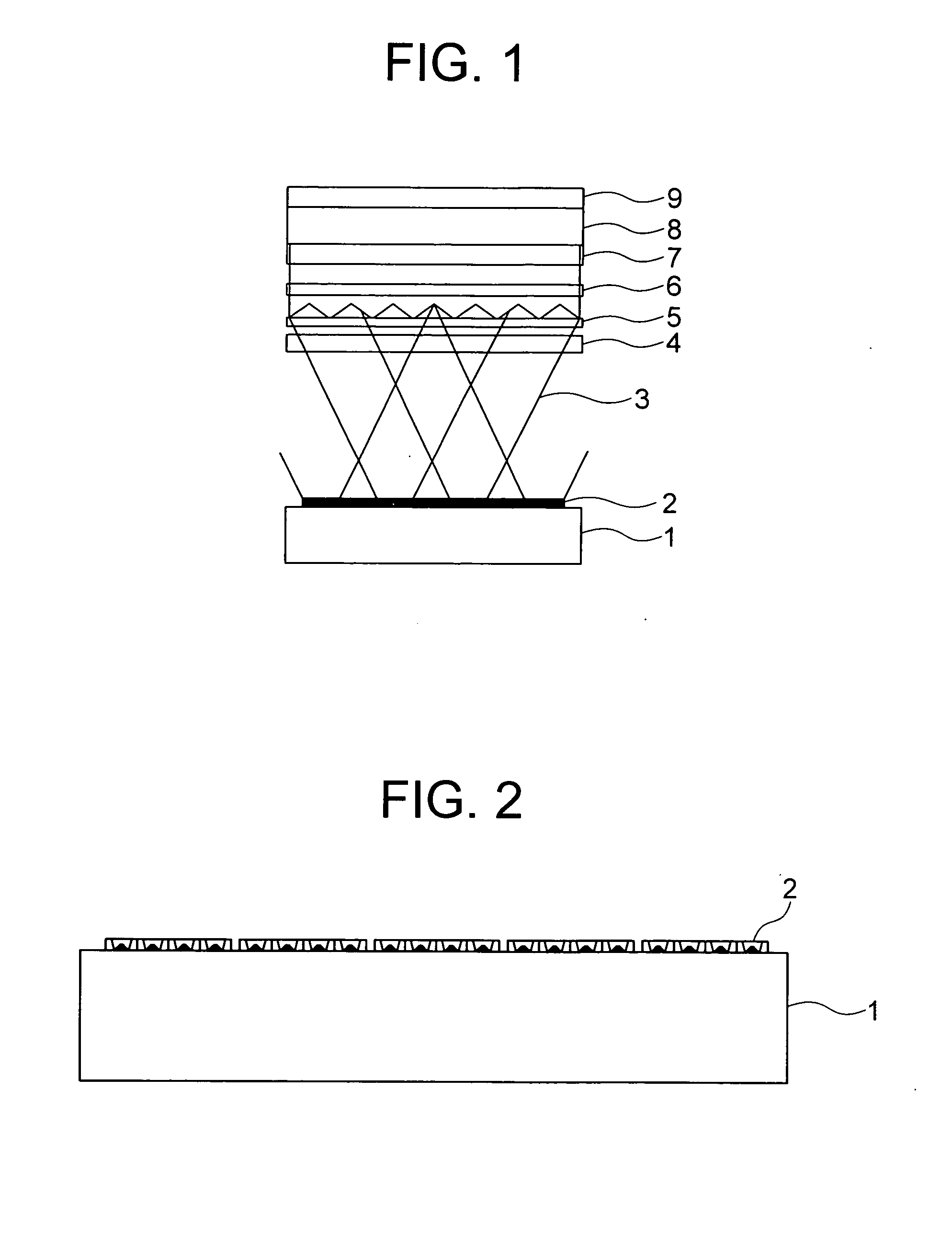
[0108] Teachings of the present invention mainly contemplate features of a light emitting diode element structure and its mounting form. Referring first to FIG. 1, there is illustrated, in sectional form, a liquid crystal display apparatus for television in which the light emitting diode element structure according to the embodiment of the invention is mounted. A module is constructed by having light emitting diode unit elements 2 carried on a backlight module housing 1. Rays of backlight 3 emitted from the light emitting diode element structure transmit through a diffusion plate 4, a positive prism sheet 5, a diffusion film 6, a lower polarization plate 7, a thin film transistor and liquid crystal panel 8 for television and an upper polarization plate 9, thereby illuminating the liquid crystal panel display apparatus.

[0109] The light emitting diode element structure and its mounting...

embodiment 2

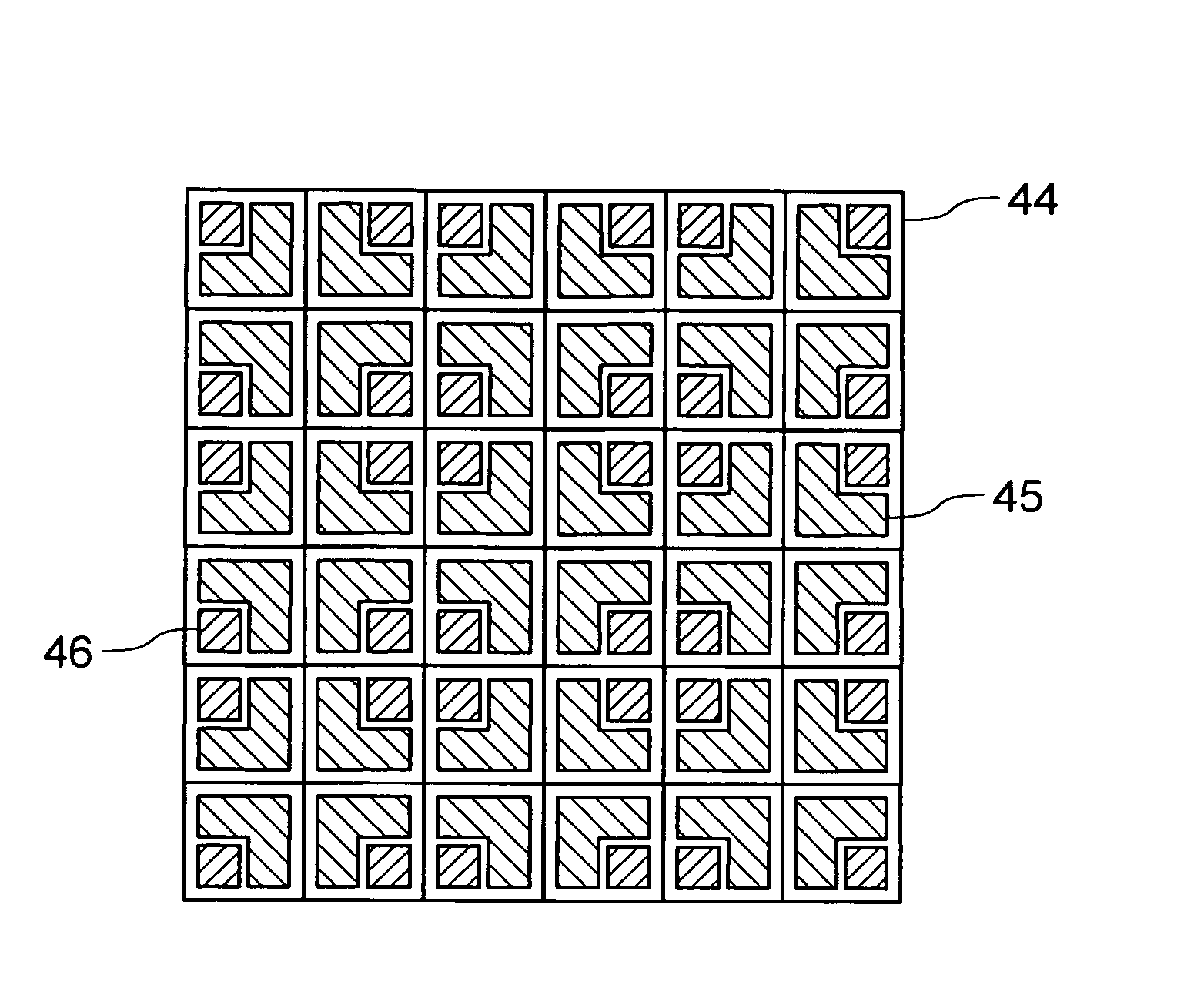
[0118] A second embodiment of the present invention will now be described with reference to FIGS. 31A to 31C. As in embodiment 1, the shape cut out of the light emitting diode element wafer can be arbitrary. The wiring substrate can be applied by making it commensurate with the electrode pattern structure of a cutout light emitting diode element structure. For example, as shown in FIGS. 31A to 31C, a light emitting diode element structure of large area can be set up by increasing the period of cut-out from the light emitting diode element wafer. It is not necessary for the electrode structure and process steps to be specifically changed to meet a large element structure. In other words, by making the electrode structure and process step commensurate with the unit element of small area, element structures having small to large areas can be produced from the same wafer. Element structures of small size and large size can be used selectively in accordance with different applications. T...

embodiment 3

[0121] A third embodiment of the invention will be described with reference to FIGS. 33 to 39.

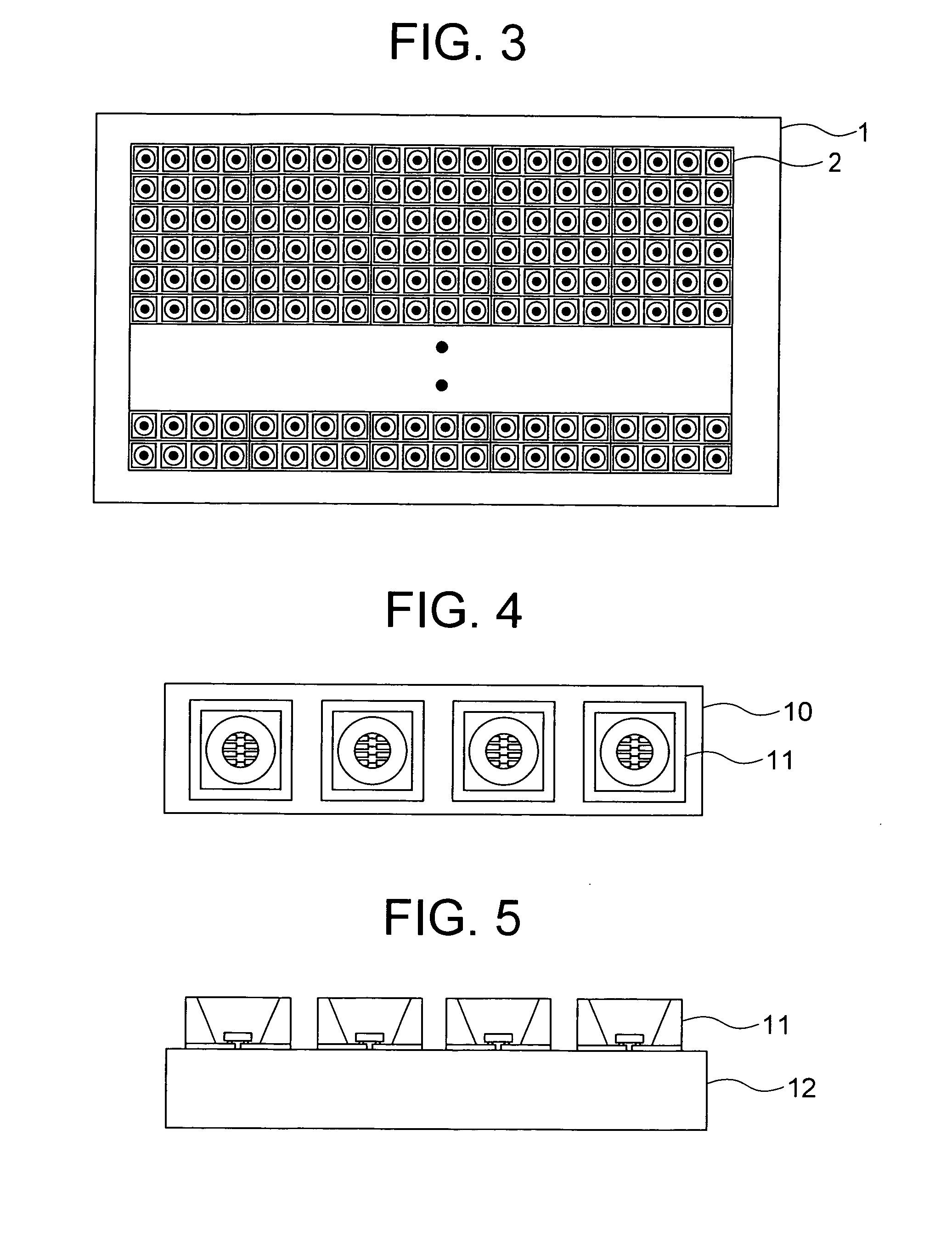
[0122] In the present embodiment, a backlight source constituting a liquid crystal panel display apparatus for cell phone is formed. A light emitting diode element structure applied to the backlight source essentially presupposes that the electrode pattern of element structure is constructed and flip chip mounting is performed as has been explained in connection with embodiment 1. The liquid crystal panel display apparatus for cell phone is constructed as illustrated in FIG. 33. In association with liquid crystal panel pixels 49, a backlight module having, as a light source, light emitting diode unit elements 50 of the invention is structured and the backlight is operated through film wire 51 and drive circuit 52. Illustrated in FIGS. 34 and 35 is a constitution in which light emitting diode unit element packages 53 of the invention are carried on a wire and film 54 and the liquid crystal ...


PUM

PropertyMeasurementUnit
breakdown voltageaaaaaaaaaa
electricalaaaaaaaaaa
light intensityaaaaaaaaaa

Abstract

A cold-cathode tube has hitherto been used as a backlight for supplying illumination to a liquid crystal television but recently, light emitting diode pieces have been used for a backlight of a large-size liquid crystal television. For the purpose of improving the emission efficiency, flip chip mounting of the light emitting diode piece is advantageous but the mounting yield is restricted by the piece size, electrode structure and wire pattern structure, facing situations having difficulties in realizing simplified mounting and reduction of costs of members. In a liquid crystal display apparatus having a liquid crystal panel, an optical system and a light source, the light source includes a light emitting element structure having positive and negative electrodes, at least one of them being plural, and wires mounted to the positive and negative electrodes through flip chip mounting by making electrical correspondence to individual regions of the positive and negative electrodes.

Description

BACKGROUND OF THE INVENTION [0001] The present invention relates to liquid crystal display apparatuses. [0002] In the liquid crystal display apparatus, a cold cathode tube has hitherto been used as a backlight source but recently, a module having a semiconductor light emitting diode (LED) element applied to the backlight source has been developed for liquid crystal televisions. In a compact liquid crystal panel for use in a cell phone, a white light source having a blue semiconductor light emitting diode element and a yellow fluorescent substance in combination has been used for backlight. But for medium and large size liquid crystal display panels, an LED backlight module is needed in which LED elements for three primary colors of red, green and blue are built in and they are controlled independently to improve the color display performance with high picture quality. [0003] In constituting the backlight module, it is important that the LED element to be mounted is highly efficient ...

Claims


Application Information

Patent Timeline
Patent Type & Authority Applications(United States)
IPC IPC(8): G02F1/1335H01L33/50H01L33/56H01L33/62
CPCG02F1/133603G02F2001/133612H01L25/0753H01L33/38H01L33/62H01L2224/48091H01L2924/00014H01L2224/16225H01L2224/48465H01L2224/16245H01L2224/45144H01L2924/00G02F1/133612H01L2924/181H01L2924/00012
Inventor TANAKA, TOSHIAKIKANEKO, HIROKIHIYAMA, IKUO
Owner PANASONIC LIQUID CRYSTAL DISPLAY CO LTD
Why Eureka
Try Eureka