Semiconductor device and method for producing the same

a semiconductor and semiconductor technology, applied in the direction of semiconductor devices, basic electric elements, electrical appliances, etc., can solve the problems of image defects, image defects, and more likely, image defects in solid-state imaging devices, etc., to suppress the generation of crystal defects, suppress the generation of image defects sufficiently, and suppress the effect of slight leakage electric curren

Inactive Publication Date: 2007-04-19
PANASONIC CORP
View PDF5 Cites 10 Cited by
  • Summary
  • Abstract
  • Description
  • Claims
  • Application Information

AI Technical Summary

Benefits of technology

[0020] With the semiconductor device according to the above-described production method, it is possible to suppress a slight leakage electric current between adjacent gates. Also, various stresses applied to a semiconductor substrate can be relieved, thereby s...

Problems solved by technology

Due to the stress caused by the larger STI step height (especially in the case where polysilicon is formed on the STIs), it is more likely that image defects occur in ...

Method used


Image

  • Semiconductor device and method for producing the same
  • Semiconductor device and method for producing the same
  • Semiconductor device and method for producing the same

Examples


Embodiment Construction

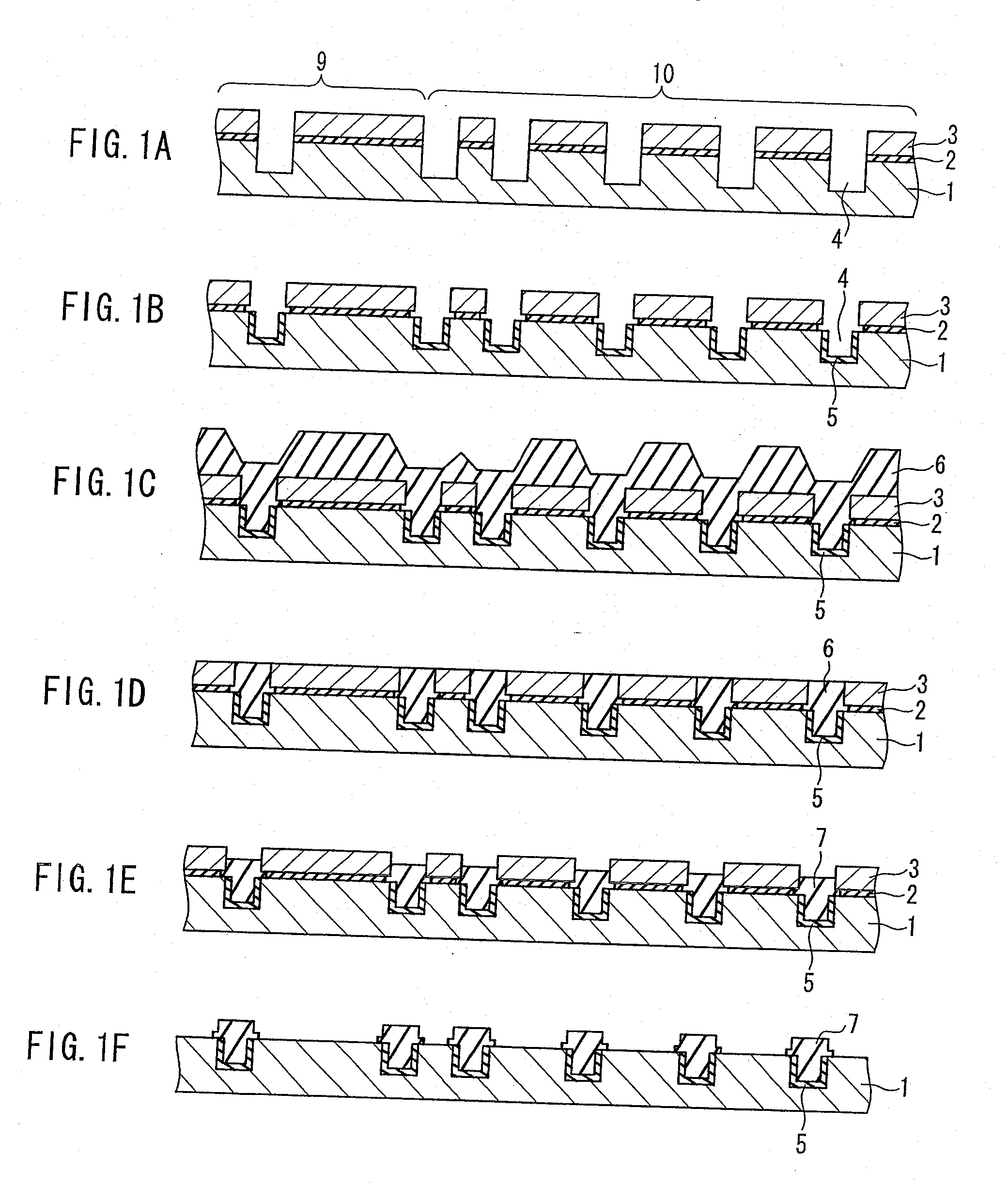
[0028] In the method for forming STIs according to the present invention, a thickness of the surface portion of the silicon nitride film removed by the CMP may be equal to or smaller than 50% of a thickness of the silicon nitride film that is formed, and a thickness of the buried oxide film removed by the wet etching may be 10% to 50% of a thickness of the silicon nitride film before the CMP.

[0029] Also, in the method for producing a semiconductor device according to the invention of the present application, the semiconductor element may be formed so as to form a photodiode for converting incident light into an electrical charge and storing it, and a MOS transistor forming a readout portion for reading out a signal charge from the photodiode, a driving portion or an amplification portion for amplifying an output signal.

[0030] The following is a specific description of an embodiment of a semiconductor device in the present invention, in particular, a solid-state imaging device as a...


PUM


Abstract

A method for forming STIs in a semiconductor substrate includes forming a protective oxide film on the semiconductor substrate and forming a silicon nitride film on the protective oxide film, performing a photolithography and a dry etching so as to penetrate the silicon nitride film and the protective oxide film and remove part of the semiconductor substrate, thus forming groove portions, forming a buried oxide film in the groove portions and on the silicon nitride film, removing the buried oxide film on the silicon nitride film and a surface portion of the silicon nitride film by a CMP, and removing part of the buried oxide film deposited in the groove portions by a wet etching. It is possible to provide a method for producing STIs capable of forming uniform STI step heights in a semiconductor device with a fine structure.

Description

BACKGROUND OF THE INVENTION [0001] 1. Field of the Invention [0002] The present invention relates to a semiconductor device, in particular, a solid-state imaging device using an active pixel MOS sensor, and a method for producing the same. [0003] 2. Description of Related Art [0004] For the element isolation in a semiconductor device, an STI (Shallow Trench Isolation) structure is used especially in the case of constituting an element using a fine pattern technology of 0.25 μm or finer. [0005] Also, with increasingly finer cells in a solid-state imaging device using an active pixel MOS sensor in recent years, the fine pattern technology of 0.25 μm or finer, namely, the element isolation of the STI structure has come to be adopted. The following is a description of such a solid-state imaging device in which an active pixel MOS sensor is mounted. [0006] The solid-state imaging device using an active pixel MOS sensor has a configuration in which a signal detected by a photodiode in eac...

Claims


Application Information

Patent Timeline
IPC IPC(8): H01L21/76H01L21/461H01L21/302
CPCH01L21/31053H01L21/76224H01L27/1463H01L27/14683H01L21/76
Inventor OCHI, MOTOTAKATSUNO, MORIKAZU
Owner PANASONIC CORP
Why Eureka
Try Eureka