Electronic module and method of assembling the same

Active Publication Date: 2007-04-26
INFINEON TECH AG
View PDF5 Cites 37 Cited by
  • Summary
  • Abstract
  • Description
  • Claims
  • Application Information

AI Technical Summary

Benefits of technology

[0083] The stack has the advantage that the area required by the two components is reduced over modules in which the two components are mounted adjacent to one another. The invention also provides a reliable module as electrical isolation between the diode and power switch is provided by the plastic encapsulation material, such as epoxy resin, which also provides the package housing of the module. The electrical isolation can be varied according to that desired by varying the distance between the adjacent contact surfaces of the stack, in this case the anode contact of the diode and the input contact of

Problems solved by technology

However, the manufacture of the semiconductor body including two or more different types of device is expensive.
However, this approach has the disadvantage that modules with two or more semiconductor components require additional electrical connections to electrically connect the different components.
This increases the inductive load and inductive losses and causes switching losses.
Additionally, two or more die attachment processes

Method used


Image

  • Electronic module and method of assembling the same
  • Electronic module and method of assembling the same
  • Electronic module and method of assembling the same

Examples


Example

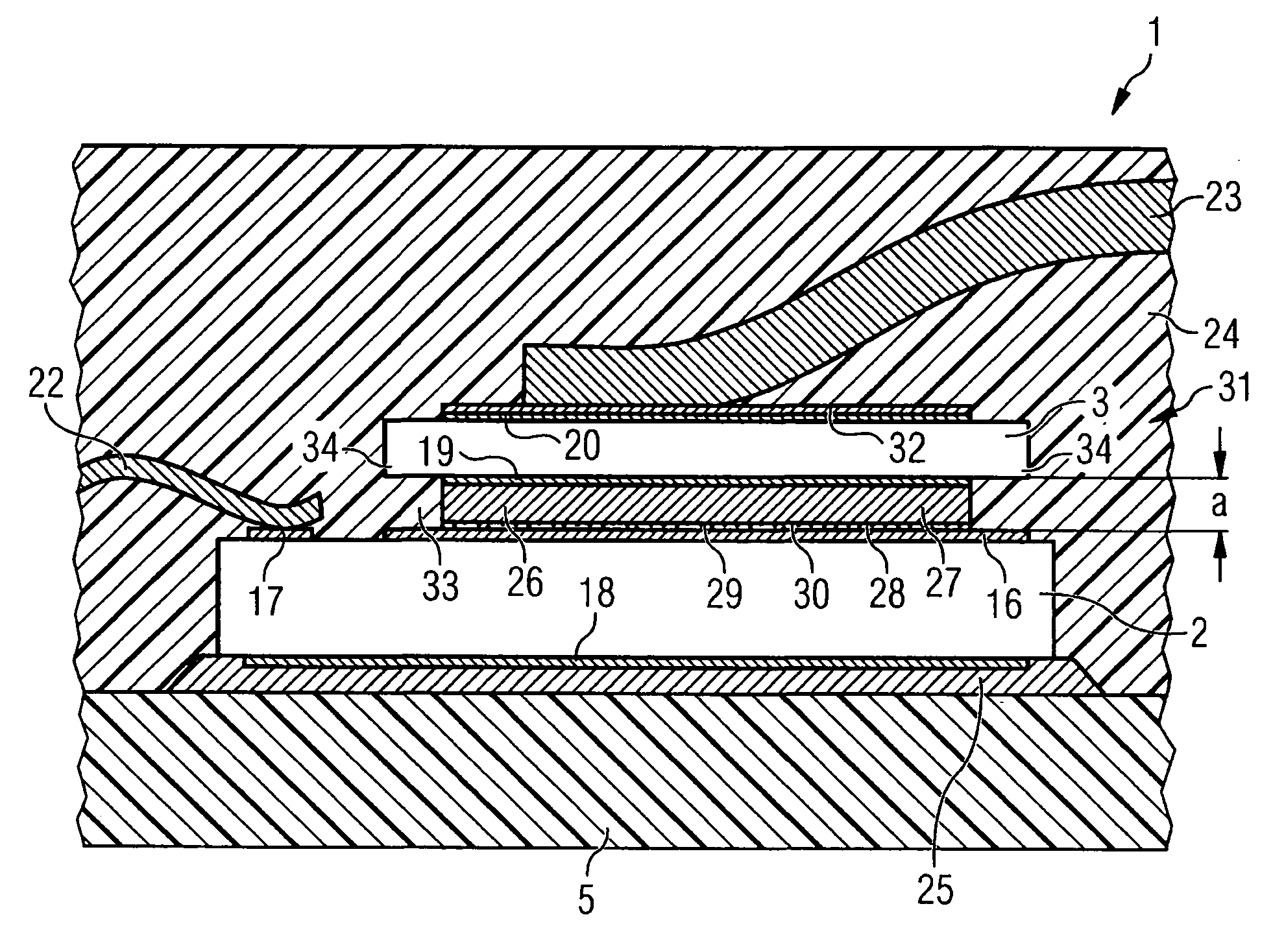
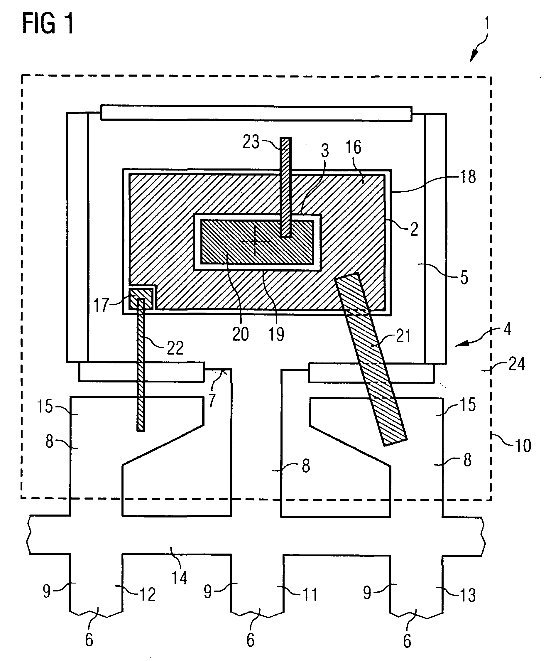
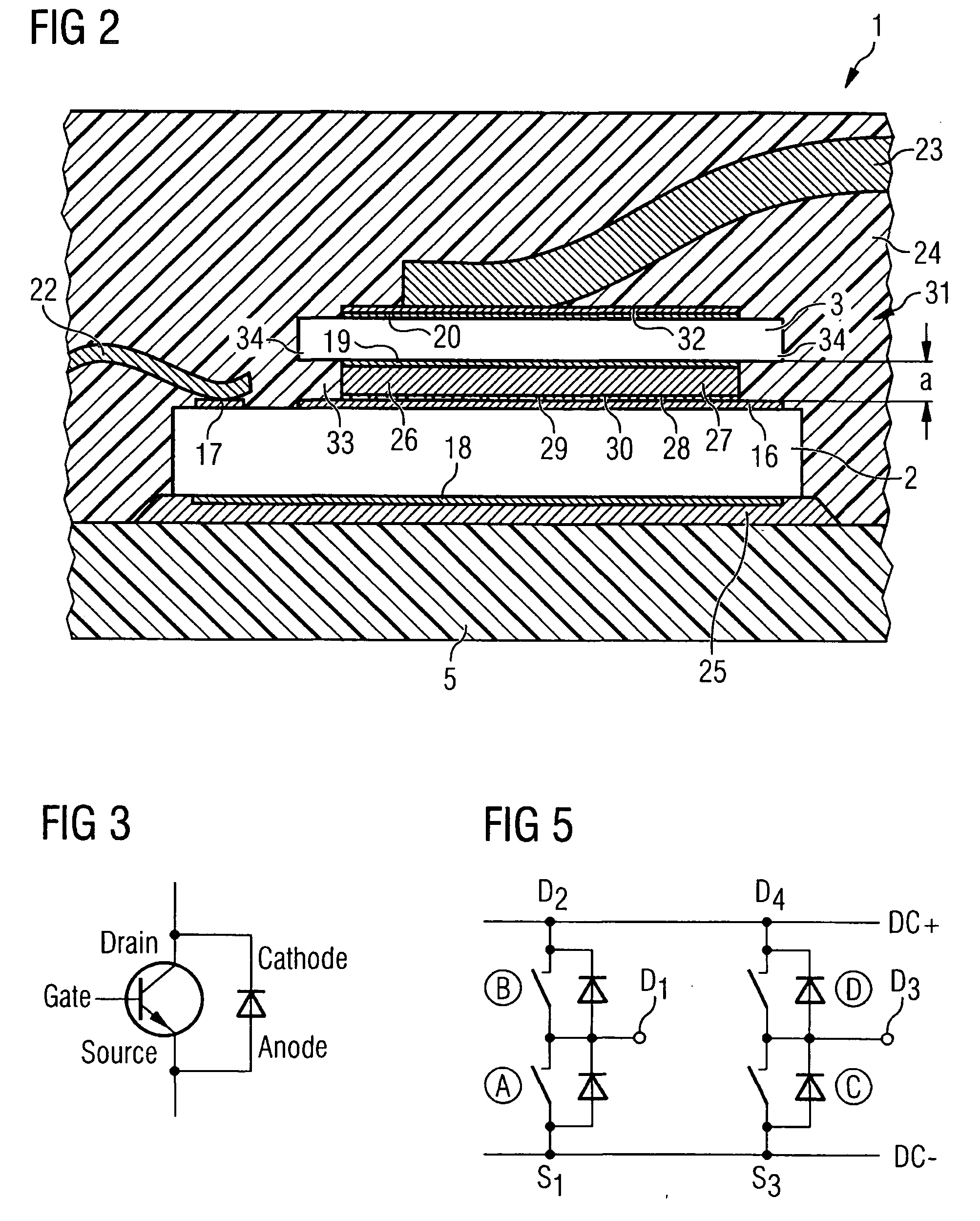
[0091]FIG. 1 shows an electronic module 1 according to a first embodiment of the invention which comprises a vertical MOSFET device 2, which provides a semiconductor power switch, and a vertical Schottky semiconductor diode 3. The electronic module 1 further comprises a leadframe 4 and package housing 10, which is indicated in FIG. 1 by the dashed line.

[0092] The leadframe 4 comprises a die pad 5, which is essentially rectangular, and three leads, or pins 6 which are arranged adjacent the long side 7 of the die pad 5. Each lead 6 has an inner portion 8, which is disposed within the package housing 10 and an outer portion 9 which is integral with the inner portion and extends outside of the package housing 10. The outer portion 9 of the leads 6 enables the electronic component 1 to be mounted on an external higher level substrate such as a printed circuit board (which is not shown in the figures) and enables the MOSFET device 2 and diode 3 to be electrically accessed from the printe...


PUM


Abstract

An electronic module includes a semiconductor power switch and a semiconductor diode. The lower side of the semiconductor power switch includes an output contact mounted on a die pad of a leadframe, and the upper side of the semiconductor power switch includes a control contact and an input contact. The anode contact of the semiconductor diode is disposed on and electrically connected to the input contact of the semiconductor power switch. The cathode contact of the diode is electrically connected with the output contact of the power semiconductor switch.

Description

FIELD OF THE INVENTION [0001] The invention relates to electronic modules, in particular to modules including at least one semiconductor power switch and at least one semiconductor diode, and to methods of assembling electronic modules. BACKGROUND [0002] Electronic circuits such as those used in switched mode applications and in control circuits for DC motors typically require a number of different semiconductor components such as transistor devices and semiconductor diodes. The circuit is typically provided by one or more electronic modules, each module typically including a number of devices. A number devices may be provided within a single module in various ways. [0003] In one approach, a single semiconductor body is provided which includes both transistor structures and semiconductor diode structures. This arrangement has the advantage that the space required by the circuit is reduced. However, the manufacture of the semiconductor body including two or more different types of de...

Claims


Application Information

Patent Timeline
IPC IPC(8): H01L23/495
CPCH01L23/49513H01L23/49524H01L23/49562H01L23/49575H01L24/33H01L24/40H01L24/41H01L24/45H01L24/49H01L24/73H01L24/83H01L2224/45015H01L2224/45124H01L2224/45144H01L2224/48091H01L2224/48247H01L2224/48472H01L2224/4903H01L2224/49051H01L2224/49171H01L2224/49175H01L2224/73265H01L2224/83801H01L2224/8382H01L2924/01005H01L2924/01013H01L2924/01028H01L2924/01029H01L2924/01047H01L2924/0105H01L2924/01078H01L2924/01079H01L2924/01082H01L2924/01327H01L2924/13055H01L2924/13091H01L2924/19043H01L2924/20757H01L2924/2076H01L2924/30107H01L2924/0132H01L2224/32245H01L24/48H01L2224/2919H01L2924/01006H01L2924/01023H01L2924/01033H01L2924/01068H01L2924/014H01L2924/0665H01L2224/29111H01L2924/15747H01L24/32H01L2924/1305H01L2924/12032H01L2924/00014H01L2924/00H01L2924/3512H01L2224/0603H01L2224/40225H01L2224/40245H01L2924/12043H01L2924/181H01L2224/8381H01L2224/83825H01L2224/37144H01L2224/84801H01L24/37H01L2224/2612H01L2224/73221H01L2924/00012
Inventor OTREMBA, RALF
Owner INFINEON TECH AG
Why Eureka
Try Eureka