Stray light compensation in ambient light sensor

Inactive Publication Date: 2010-03-11
SHARP KK
View PDF23 Cites 51 Cited by
  • Summary
  • Abstract
  • Description
  • Claims
  • Application Information

AI Technical Summary

Benefits of technology

[0173]One advantage of a stray light compensation method embodying the present invention is that it avoids the requirement of having to subtract the current measured in the (main) reference photodiode from the current measured in the detection photodiode.
[0174]This advantage applies particularly to operation in situations where the ambient light level is small in comparison to the stray light level, where the operation of subtracting two very similar currents may result in a considerable error in the final result, particularly if the two photodiodes are not well matched.
[0175]A second advantage of an embodiment of the present invention, closely related to the first, is that both the detection sensor element is biased in its most sensitive region of operation, i.e. the ratio of the current generated when the ambient light level is non-zero to the current when the ambient light level is zero is maximised. As a result of this the effects of any mismatch in the leakage current of the detection and referenc

Problems solved by technology

If the photocurrent is smaller than the leakage current then it becomes difficult to detect.
Accordingly, an ambient light sensor whose sensing element is a thin-film polysilicon photodiode is likely to exhibit poor sensitivity, especially at higher operating temperatures.
A photodiode is not the only possible photosensor device for converting incoming light to current.
In practice, accurate implementation of the circuit of FIG. 7 may be difficult since the circuit components are non ideal.
As well as obtaining a sufficiently high ratio of photocurrent to leakage current, a further practical difficulty in many applications is the requirement to compensate the light measuring circuit to offset for the effects of unwanted (“stray”) light.
The effects of stray light are a particular concern when the light sensor is integrated into the display as, even with careful design, minimising the stray light to levels comparable to or below the lowest detectable ambient light levels may in practice be very difficult.
The disadvantage of these schemes lies in the complexity of their practical circuit implementations and the amount of processing power that they require in order to perform the compensation.
In particular this means that these schemes would not be well suited to integration into an AMLCD, due to both the number of and the performance requirements of the circuit components that would need to be monolithically integrated.
An additional disadvantage is that these s

Method used


Image

  • Stray light compensation in ambient light sensor
  • Stray light compensation in ambient light sensor
  • Stray light compensation in ambient light sensor

Examples


Example

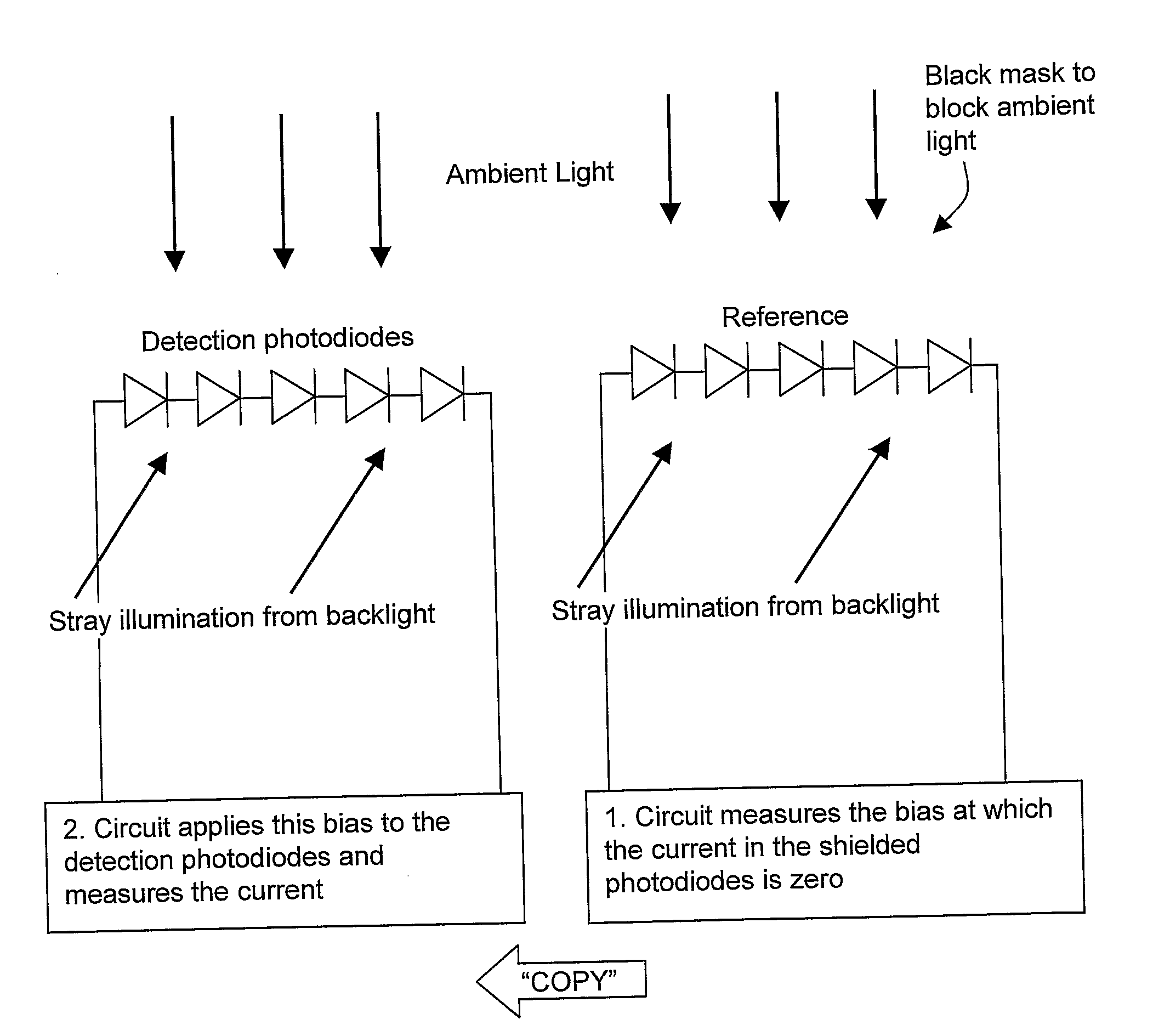
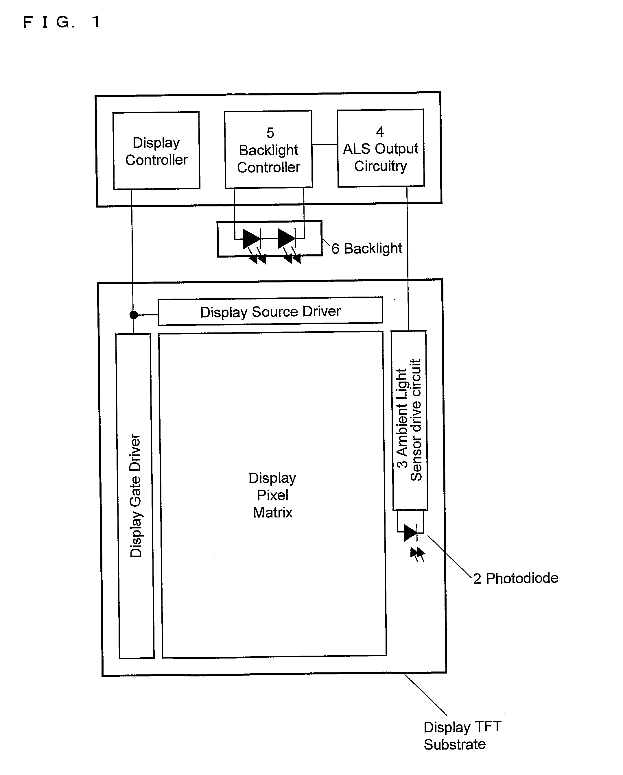
[0220]The first embodiment consists of a light sensor circuit comprising of the following elements:

[0221]A detection photosensor element which is exposed to ambient light

[0222]A reference photosensor element which is shielded from ambient light.

[0223]A measurement circuit which is connected to the detection and reference photosensor elements.

[0224]The detection and reference photodiodes may be designed to be nominally identical and to be both electrically and optically well matched.

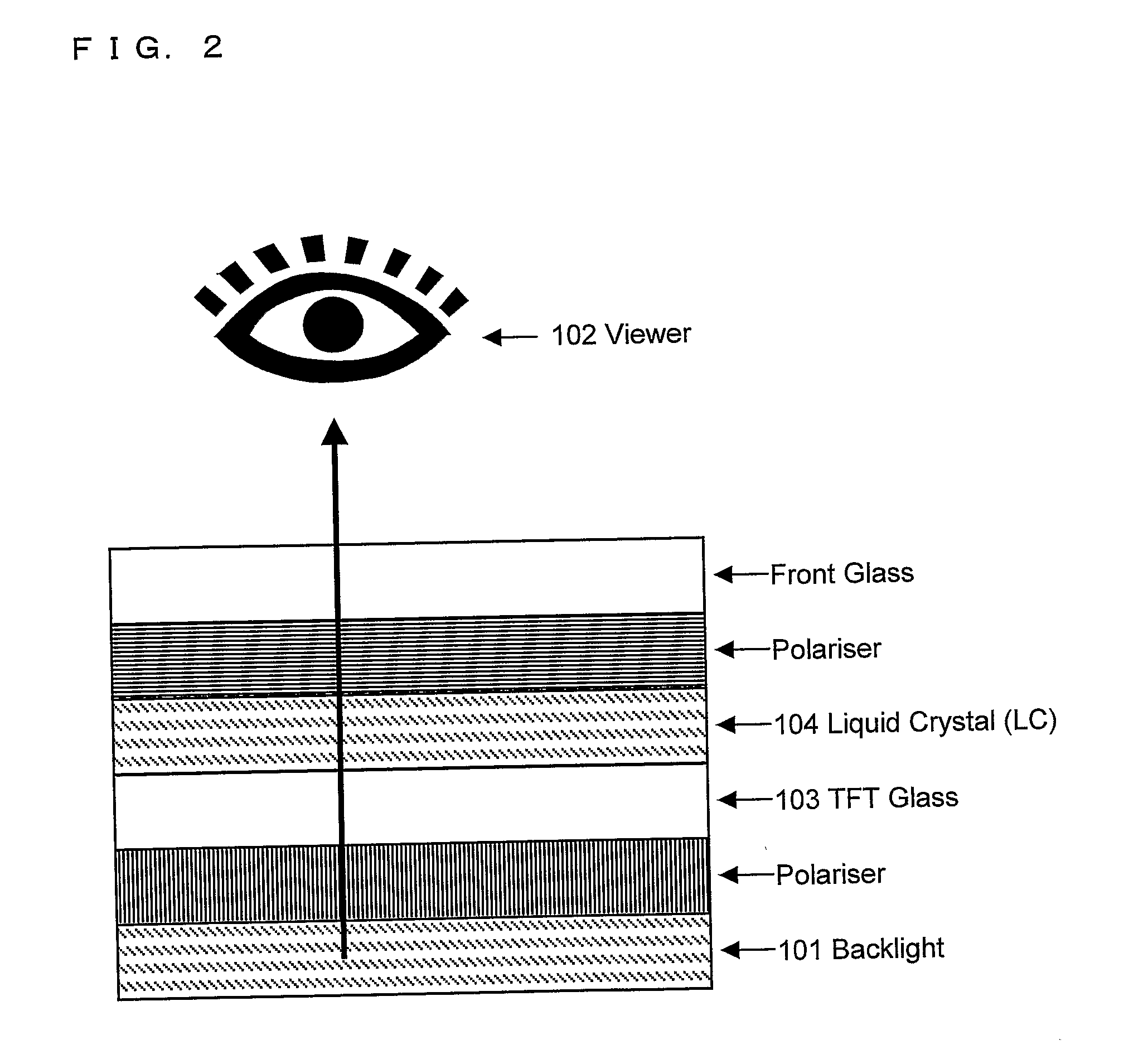
[0225]A light blocking layer is used as in FIG. 12 so that the detection photodiode is exposed to both ambient and stray light, and the reference photodiode is just exposed to ambient light.

[0226]The operation of the light sensor circuit is as follows:

[0227](i) The measurement circuit measures the bias that needs to be applied between the terminals of the reference photosensor element such that a current substantially equal to zero flows through the reference photosensor element. The bias that the measure...

Example

[0247]The second embodiment consists of a light sensor comprising the following elements:

[0248]A detection photosensor element which is exposed to ambient light

[0249]A reference photosensor element which is shielded from ambient light.

[0250]A measurement circuit which is connected to the detection and reference photosensor elements.

[0251]A subtraction circuit for storing and subtracting two digital signals

[0252]The operation of the light sensor circuit of this embodiment is as follows:

[0253](i) The measurement circuit measures the bias that needs to be applied between the terminals of the reference photosensor element such that a current substantially equal to zero flows through the reference photosensor element. The bias that the reference sensor circuit needs to apply in order to achieve this is then substantially equal to the open circuit bias of the reference photosensor element VOC(A).

[0254](ii) The measurement circuit measures the current ID that flows between the two terminal...

Example

[0287]The third embodiment of the invention consists of a light sensor circuit comprising of the following elements:

[0288]A detection photosensor element which is exposed to ambient light.

[0289]A first reference photosensor element which is shielded from ambient light.

[0290]A second reference photosensor element which is shielded from ambient light.

[0291]A measurement circuit which is connected to the detection and reference photosensor elements.

[0292]The operation of the light sensor circuit of this embodiment is as follows:

[0293](i) The measurement circuit measures the bias that needs to be applied between the two terminals of the first reference photosensor element such that a current substantially equal to zero flows through the first reference photosensor element. The bias that the measurement circuit needs to apply in order to achieve this is then substantially equal to the open circuit bias of the first reference photosensor element VOC(A).

[0294](ii) The measurement circuit t...


PUM


Abstract

A method is provided of compensating for stray light in a light sensor having a detection photosensor (7) and a reference photosensor (20), the reference photosensor (7) being for use in compensating for stray light falling on the detection photosensor (20). The method comprises using the reference photosensor (20) at least in part to determine a bias voltage applied to the detection photosensor (7). Based on this method, a display device is provided comprising a backlight and a light sensor for determining an ambient light level with the effects of stray light from the backlight substantially removed, with means provided for controlling the intensity of the backlight in dependence upon the determined ambient light level.

Description

TECHNICAL FIELD[0001]The present invention relates to stray light compensation in light sensor devices. The present invention relates particularly but not exclusively to photosensor devices that are integrated into an active matrix liquid crystal display (AMLCD). For example, the present invention finds particular application in the integration of an ambient light sensor (ALS) on the AMLCD display substrate.BACKGROUND ART[0002]FIG. 2 of the accompanying drawings shows a simplified cross section of a typical AMLCD. The backlight is a light source used to illuminate the display. The transmission of light through the display, from the backlight 101 to the viewer 102, is controlled by the use of electronic circuits made from thin film transistors (TFTs). The TFTs are fabricated on a glass substrate (known as the TFT glass 103) and are operated so as to vary the electric field through the Liquid Crystal (LC) 104 layer. This in turn varies the optical properties of the LC material and thu...

Claims


Application Information

Patent Timeline
IPC IPC(8): G09G3/36G01J1/16H05B37/02
CPCG02F1/13318G02F2001/133626H01L31/153H01L31/03682H01L31/105H01L31/02164G01J1/4228G01J1/44G01J1/46G01J2001/444G01J2001/446G02F1/133626G09G3/3406H01L31/02019
Inventor HADWEN, BENJAMIN JAMESBROWN, CHRISTOPHER JAMESCOULSON, MICHAEL PAULZEBEDEE, PATRICK
Owner SHARP KK
Why Eureka
Try Eureka