ESD protection circuit

Active Publication Date: 2019-12-05
ANPEC ELECTRONICS CORPORATION
View PDF0 Cites 1 Cited by
  • Summary
  • Abstract
  • Description
  • Claims
  • Application Information

AI Technical Summary

Benefits of technology

The present invention provides an electrostatic discharge protection circuit that reduces the area required for an internal circuit during circuit layout design, while achieving electrostatic protection. This is achieved through the use of a control circuit and high voltage transistor that work together to limit the voltage received by the internal circuit during an electrostatic discharge (ESD) event. The high voltage transistor operates in a linear region, ensuring relatively small conductive resistance and not affecting normal operation.

Problems solved by technology

The electrostatic discharge pulses can damage the integrated circuits of the chips.
However, under the premise of following the static protection rules, a large area is required in the circuit layout design, the time cost of the layout design may be increased, and furthermore, the layout must be redesigned for certain fixed circuit modules.
Therefore, how the area required for the internal circuit can be reduced during the circuit layout design by improving the electrostatic circuit architecture to overcome the above-mentioned defects has become an important issue in the art.

Method used


Image

  • ESD protection circuit
  • ESD protection circuit
  • ESD protection circuit

Examples


first embodiment

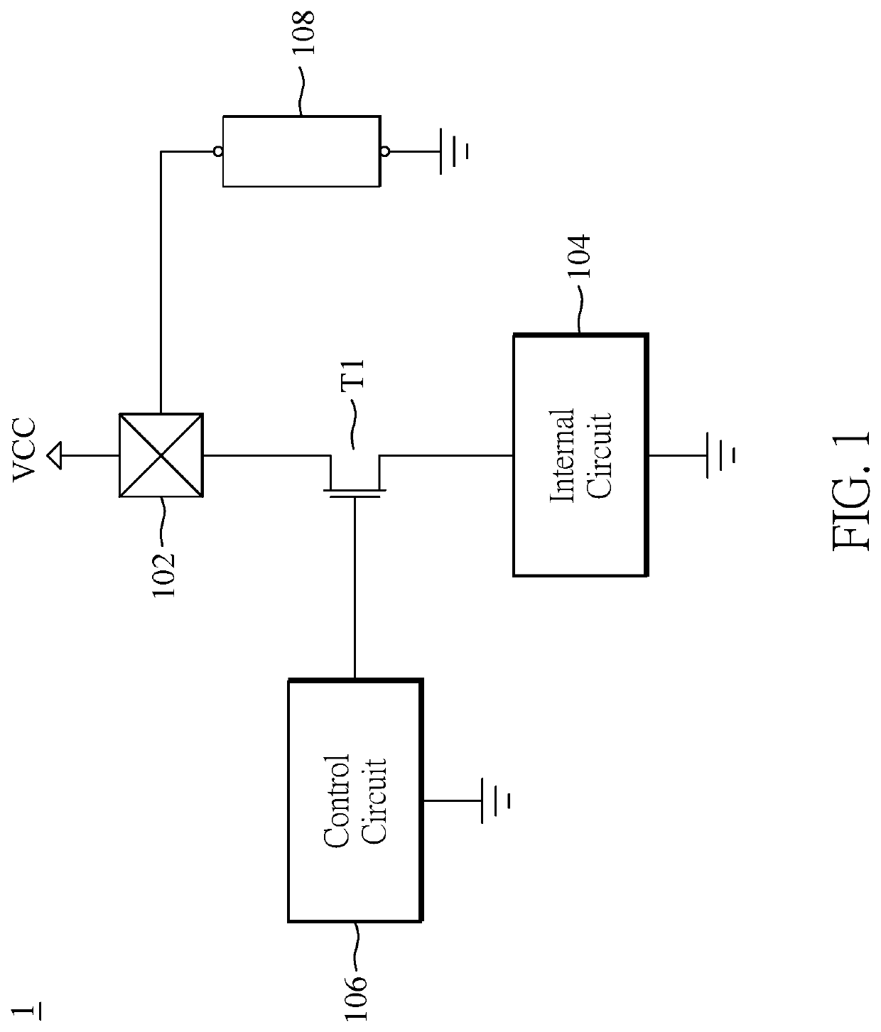
[0023]Reference is now made to FIG. 1, which is a circuit layout of an electrostatic discharge protection circuit according to a first embodiment of the present disclosure. As can be seen from FIG. 1, the first embodiment of the present disclosure provides an electrostatic discharge protection circuit 1 including a pad 102, an internal circuit 104, a control circuit 106, an electrostatic protection component 108, and a first high voltage transistor T1.

[0024]In detail, the pad 102 may receive the power supply voltage VCC from the high voltage source, and the first end of the first high voltage transistor T1 is coupled to the pad 102, the second end of the first high voltage transistor T1 is coupled to the internal circuit 104, and the first high voltage transistor T1 has a control terminal for controlling the first high voltage transistor T1 to be switched between ON and OFF states according to the voltage supplied thereto.

[0025]The electrostatic protection element 108 has one end co...

second embodiment

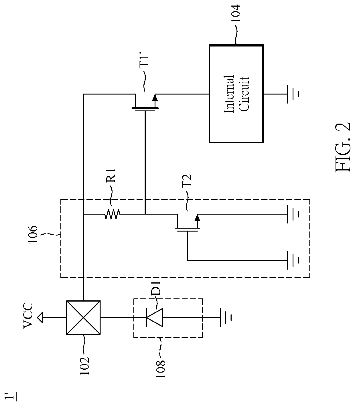
[0029]Reference is now made to FIG. 2, which is a circuit layout of an electrostatic discharge protection circuit according to a second embodiment of the present disclosure. As can be seen from FIG. 2, the second embodiment of the present disclosure provides an electrostatic discharge protection circuit 1′ including a pad 102, an internal circuit 104, a control circuit 106, an electrostatic protection component 108, and a first high voltage transistor T1′. In the present embodiment, like elements are denoted by like reference numerals, and repeated description is omitted.

[0030]The ESD protection component 108 includes an ESD diode D1, and the ESD diode D1 has a positive pole coupled to the ground terminal and a negative pole coupled to the pad 102. In detail, the electrostatic protection component 108 can be, for example, the ESD diode D1, which is coupled in parallel within the circuit. When the circuit works normally, it is in an OFF state (high resistance state), which does not a...

third embodiment

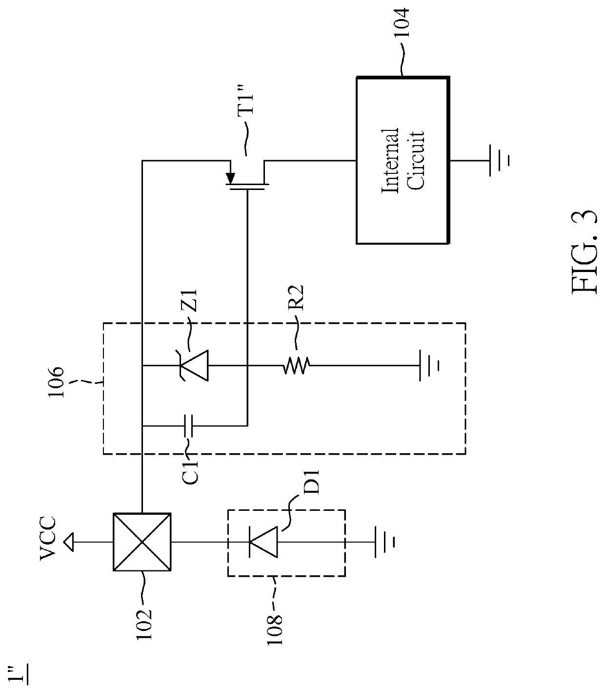
[0036]Reference is now made to FIG. 3, which is a circuit layout of an electrostatic discharge protection circuit according to a third embodiment of the present disclosure. As can be seen from FIG. 3, the third embodiment of the present disclosure provides an electrostatic discharge protection circuit 1″ including a pad 102, an internal circuit 104, a control circuit 106, an electrostatic protection component 108, and a first high voltage transistor T1″. In the present embodiment, like elements are denoted by like reference numerals, and repeated description is omitted.

[0037]Similarly, the electrostatic protection component 108 can be, for example, the ESD diode D1, which is coupled in parallel within the circuit. When the circuit works normally, it is in an OFF state (high-impedance state), which does not affect the normal operation of the circuit, and when the circuit has an abnormal overvoltage and reaches its breakdown voltage, the ESD diode D1 can be quickly changed from a high...


PUM


Abstract

An electrostatic discharge protection circuit includes an internal circuit, a pad, a first high voltage transistor, an electrostatic protection element and a control circuit. A first terminal of the first high voltage transistor is coupled to the pad, a second terminal of the first high voltage transistor is coupled to the internal circuit and includes a control terminal. The electrostatic protection element has one end coupled to the first end of the first high voltage transistor and the other end grounded. The control circuit is coupled between the control terminal of the first high voltage transistor and the ground terminal. The control circuit is configured to control the first high voltage transistor to turn off when the pad receives an electrostatic voltage.

Description

CROSS-REFERENCE TO RELATED PATENT APPLICATION[0001]This application claims the benefit of priority to Taiwan Patent Application No. 107119174, filed on Jun. 4, 2018. The entire content of the above identified application is incorporated herein by reference.[0002]Some references, which may include patents, patent applications and various publications, may be cited and discussed in the description of this disclosure. The citation and / or discussion of such references is provided merely to clarify the description of the present disclosure and is not an admission that any such reference is “prior art” to the disclosure described herein. All references cited and discussed in this specification are incorporated herein by reference in their entireties and to the same extent as if each reference was individually incorporated by reference.FIELD OF THE DISCLOSURE[0003]The present disclosure relates to an electrostatic discharge (ESD) protection circuit, and more particularly to an electrostati...

Claims


Application Information

Patent Timeline
IPC IPC(8): H01L27/02H02H9/04
CPCH02H9/046H01L27/0266H01L27/0255H02H9/04H01L27/0251H01L27/0285
Inventor CHEN, KUN-MINCHU, CHIEN-LUN
Owner ANPEC ELECTRONICS CORPORATION
Why Eureka
Try Eureka