Printed wiring board

Active Publication Date: 2007-05-03
IBIDEN CO LTD
View PDF13 Cites 56 Cited by
  • Summary
  • Abstract
  • Description
  • Claims
  • Application Information

AI Technical Summary

Benefits of technology

[0009] Further, in the embodiment of the present invention, the surface of the flattened solder resist layer can be further roughened, and it is desirable that surface roughness of the roughened

Problems solved by technology

Therefore, the flip-chip type has, in case of repeating temperature change with heat generation, the possibility of destroy

Method used


Image

  • Printed wiring board
  • Printed wiring board
  • Printed wiring board

Examples


example 1

(1) Manufacture of Printed Wiring Board

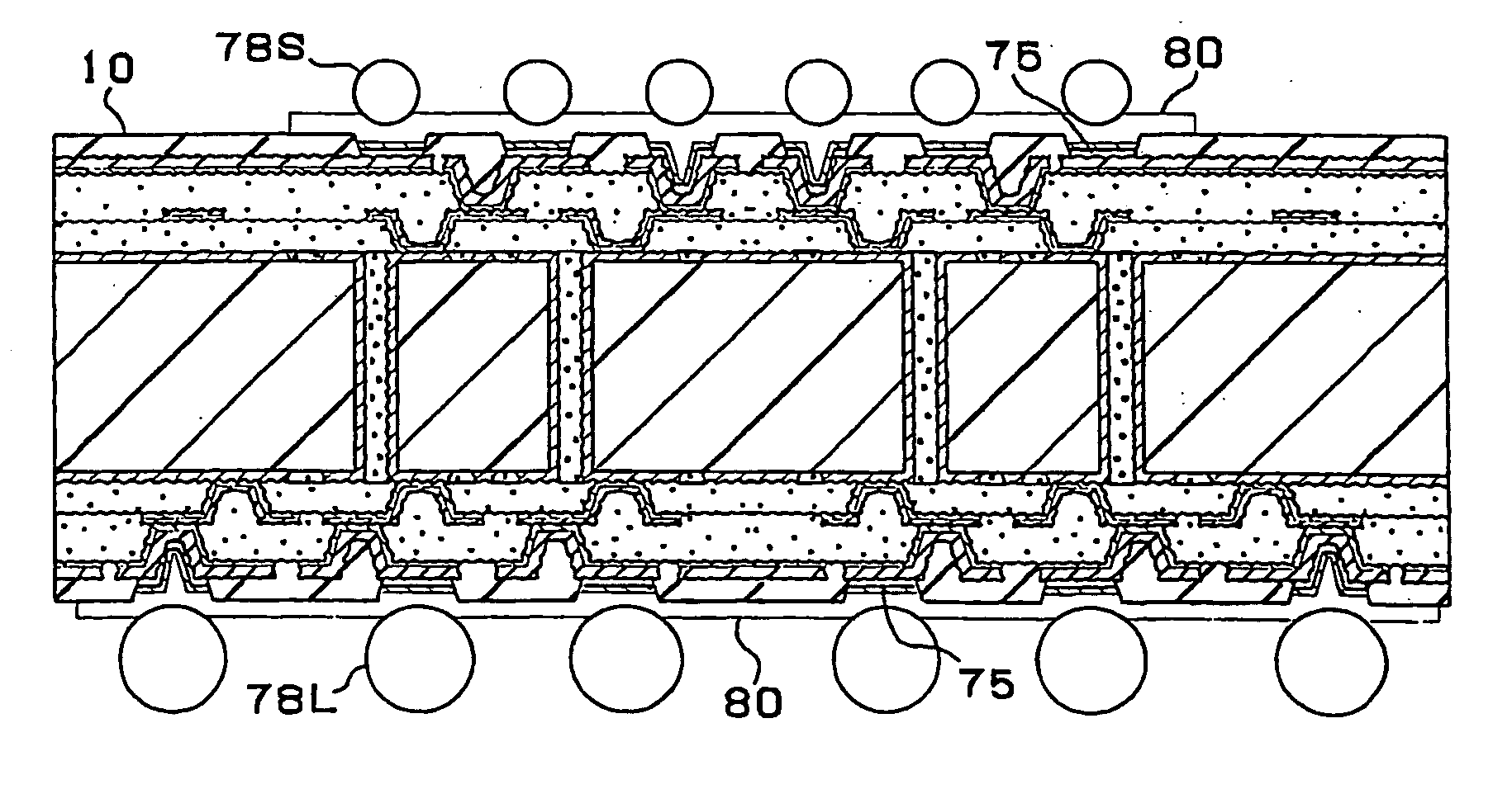
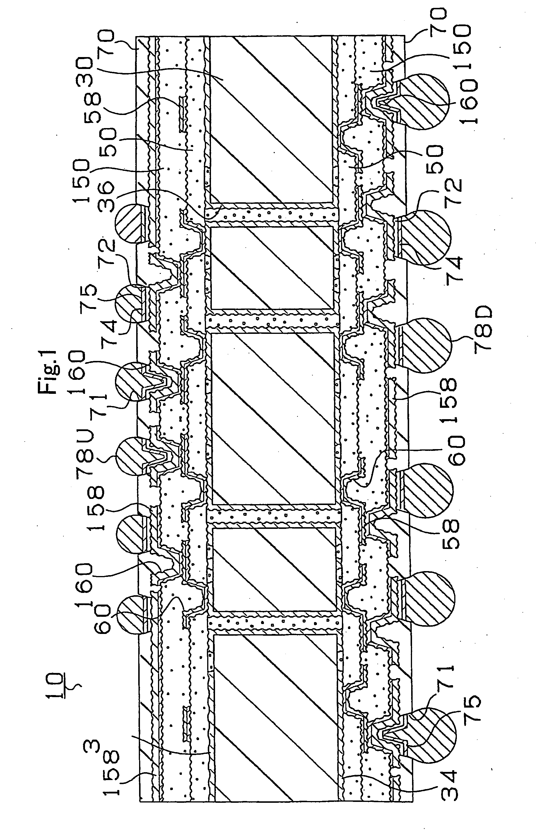
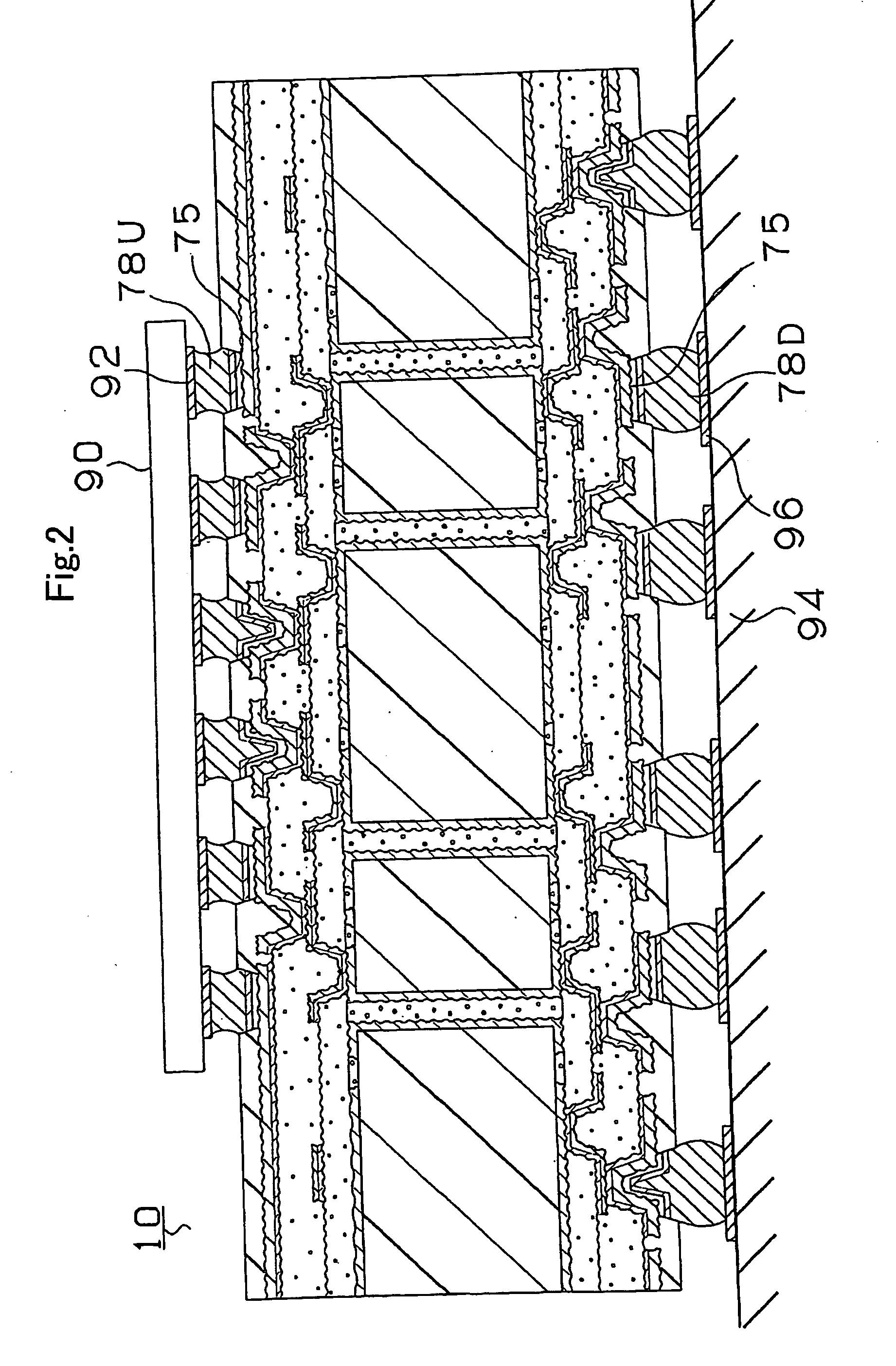
[0075] As starting material, a double sided copper-clad laminate (e.g. “MCL-E-67” made by Hitachi Chemical) is used, and on this substrate are formed a through-hole conductor and a conductor circuit by a known method. Thereafter, insulating layers and conductor circuit layers are alternately laminated by a known method (e.g. described in a book entitled “Build-up multilayer printed wiring board” (Kiyoshi Takagi) published by Nikkan Kogyo Shinbunsha on Jun. 20, 2000, and the content of this book is incorporated herein by reference in its entirety), and in the outermost conductor circuit layer, a group of connecting pads for mounting IC chips consisting a grid-like arrangement having thickness: 20 μm, diameter (conductor pad diameter): 150 μm, pitch: 200 μm, number: 50×40 (pieces) is formed within a connecting pad region of 150 mm2.

[0076] A dimension of the region for forming these connecting pads was 150 mm2. Such connecting pad are formed by...

example 2

[0095] Except that the printing condition (mesh of the screen and printing speed) of the solder resist is regulated, film thickness of the solder resist is made 15 μm and the solder ball having a diameter of 140 μm is mounted with the use of the ball aligning mask having an opening diameter of 160 μm, a printed wiring boards is manufactured in the same manner as in Example 1. As a result, the minimum value of the solder bump height becomes 63 μm and the maximum value thereof becomes 68 μm.

example 3

[0096] Except that the printing condition (mesh of screen and printing speed) of the solder resist is regulated, film thickness of the solder resist is made 15 μm and the solder ball having a diameter of 135 μm is mounted with the use of the ball aligning mask having an opening diameter of 155 μm, a printed wiring board is manufactured in the same manner as in Example 1. As a result, the minimum value of the solder bump height becomes 65 μm and the maximum value thereof becomes 70 μm.


PUM

PropertyMeasurementUnit
Lengthaaaaaaaaaa
Thicknessaaaaaaaaaa
Surface roughnessaaaaaaaaaa

Abstract

A printed wiring board comprises a wiring substrate provided with at least one conductor circuit, a solder resist layer formed on the surface of the wiring substrate, covering the at least one conductor circuit, conductor pads formed on a part of the at least one conductor circuit exposed from respective openings provided in the solder resist layer for mounting electronic parts, and solder bumps formed on the respective conductor pads. Connection reliability and insulation reliability are easily improved by making the ratio (H/D) of a height H from solder resist layer surface the solder bump to an opening diameter of the opening about 0.55 to about 1.0 even in narrow pitch structure under the pitch of the opening provided in the solder resist layer of about 200 μm or less.

Description

[0001] The present invention is an application claiming priority of JP 2005-192862 filed with Japanese Patent Office on Jun. 30, 2005, and the disclosure of which is incorporated herein by reference in its entirety. TECHNICAL FIELD [0002] The present invention relates to a printed wiring board for mounting electronic parts such as capacitors, IC and the like on the outer layer, more particularly, a printed wiring board adaptable to narrow pitching of solder bump for mounting electronic parts. BACKGROUND ART [0003] Recent years, high performance is remarkable in electronics represented by portable telephones and communication terminals. And, for these electronics is used a printed wiring board having IC chips mounted thereon. As a method of mounting IC chips on a printed wiring board, a flip chip type of directly mounting IC chips on the surface of a printed wiring board is widely employed. As such a printed wiring board, there has been known the one comprising a core substrate, a bu...

Claims


Application Information

Patent Timeline
IPC IPC(8): H01L23/48H01L23/52H01L29/40
CPCH01L21/4853Y10T29/49165H01L23/49816H01L23/49822H01L24/16H01L2224/13099H01L2224/16H01L2924/01011H01L2924/01015H01L2924/0102H01L2924/01027H01L2924/01029H01L2924/0103H01L2924/01033H01L2924/01038H01L2924/01061H01L2924/01074H01L2924/01078H01L2924/01079H01L2924/01082H01L2924/01088H01L2924/14H01L2924/15311H01L2924/19041H05K3/3452H05K3/3478H05K2201/0191H05K2201/099H05K2203/041H05K2203/0557H01L2924/01005H01L2924/01006H01L2924/01019H01L2924/01023H01L2924/01047H01L2924/014H01L2224/81192H01L2224/11334H01L2224/16235Y10T29/49144Y10T29/49117Y10T29/49126Y10T29/49124Y10T29/4913H01L23/49811H01L2224/05568H01L2224/05573H01L2924/00014H01L2924/12042H01L2924/181H01L2924/00H01L2224/05599H05K3/28H05K3/34
Inventor KAWAMURA, YOICHIROSAWA, SHIGEKITANNO, KATSUHIKOTANAKA, HIRONORIFUJII, NAOAKI
Owner IBIDEN CO LTD
Why Eureka
Try Eureka