Wafer inspection data handling and defect review tool

a technology of defect detection and data processing, applied in the field of defect detection operation, can solve the problems of reducing operational efficiency, affecting the efficiency of inspection, and affecting the accuracy of inspection results, so as to reduce the time it takes for inspection and extract the defect. , the effect of reducing nois

Inactive Publication Date: 2007-05-10
HITACHI HIGH-TECH CORP
View PDF10 Cites 35 Cited by
  • Summary
  • Abstract
  • Description
  • Claims
  • Application Information

AI Technical Summary

Benefits of technology

[0013] It is therefore an object of the invention to achieve higher efficiency in defect extraction while reducing the time it takes for the determination of an inspection condition that is set in a wafer inspection tool for detecting defects. For this purpose, the invention allows a defect detected by a wafer inspection tool to be captured by a defect review tool reliably.
[0014] In accordance with the invention, a review image in which a defect is reliably captured is easily obtained as information guiding the determination of such a defect inspection condition that a DOI (Defect of Interest) can be detected while reducing noise and improving the average defect capture ratio. For this purpose, the defect review condition in the defect review tool is varied depending on the defect attributes provided by the wafer inspection tool so as to optimize the reviewing process. In this way, a detected defect can be surely captured in the review image provided by the defect review tool, and the reliability of defect inspection condition determination can be improved.
[0015] Specifically, based on a setting such that RDC attributes can be outputted by the wafer inspection tool, a data handling tool is prepared that is connected to both the wafer inspection tool and the defect review tool via a network. The data handling tool processes the data provided by the wafer inspection tool and the defect review tool, and causes the defect ID of the result of inspection, which is performed a plurality of times with the same or varying inspection condition, a corresponding image data, and RDC attributes to be displayed and arranged. Data concerning the same defect is grouped by collating the coordinates, and such defect information (coordinates and attributes) is outputted to the defect review tool. Based on the information, the defect review tool modifies the review condition either manually or automatically, and acquires an image using such a review condition under which even a defect that is particularly difficult to observe can be captured in the image. The thus obtained image is then fed back to the data handling tool and displayed alongside the information provided by the wafer inspection tool. In this way, an optimum wafer inspection condition can be determined in a short time. The data handling tool may be integrally constructed with the defect review tool.
[0016] In accordance with the invention, defect attributes, such as the signal level of a defect, for example, are outputted to the defect review tool, and the review conditions of the defect review tool are optimized on the basis of that information. This allows the capture of an image of a very small defect that has been heretofore difficult to obtain. The image is then displayed alongside the information outputted by the wafer inspection tool, whereby the time it takes for the optimization of the inspection conditions for DOI detection can be reduced.

Problems solved by technology

Further, as a result of the increase in the sensitivity of wafer inspection tools, the influence of noise has also increased, resulting in the total number of defects that are detected sometimes exceeding several tens of thousands or more.
This has led to a very large number of defects whose shapes need to be confirmed using a defect review tool in a review operation.
It has also led to an increase in the number of cases where no defects can be found by the review operation, resulting in a decrease in operational efficiency.
In addition, there has been an explosive increase in the volume of information that needs to be fed back for the purpose of inspection and RDC condition determination in order to reduce such noise, making it ever more difficult to determine inspection conditions accurately.
It has also been difficult to set sensitivity to such a level that no noise that does not need to be detected in actual defect detection would be detected.
However, defects having low signal levels upon defect detection are so small that their review is difficult.
Thus, there are many defects of which identification is difficult and which cause a decrease in yield.
It is becoming increasingly difficult to review such defects and to distinguish noise from defects accurately.

Method used


Image

  • Wafer inspection data handling and defect review tool
  • Wafer inspection data handling and defect review tool
  • Wafer inspection data handling and defect review tool

Examples


Embodiment Construction

[0029] In the following, an embodiment of the invention will be described with reference to the drawings, where the invention is applied to a semiconductor production line.

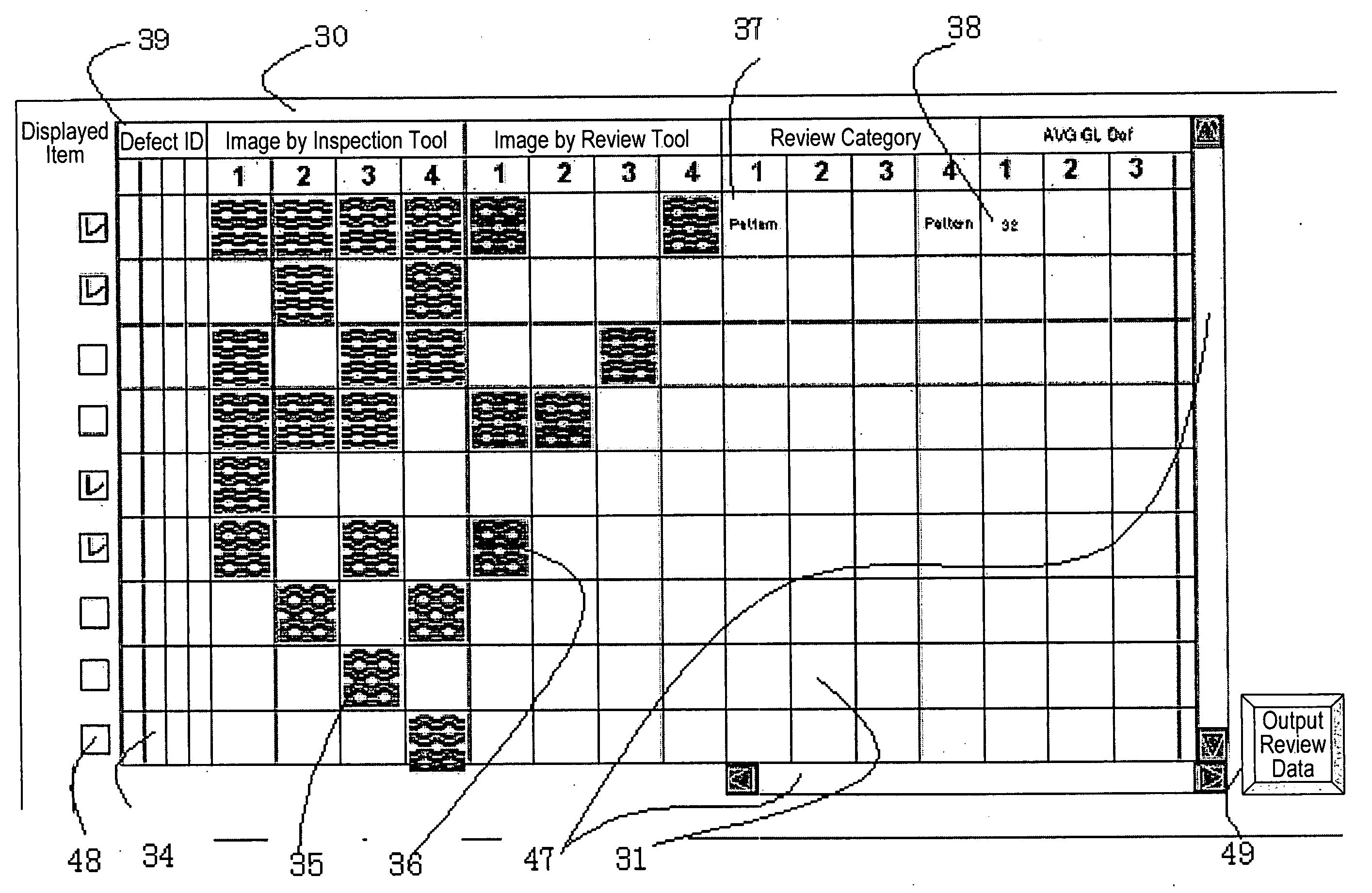
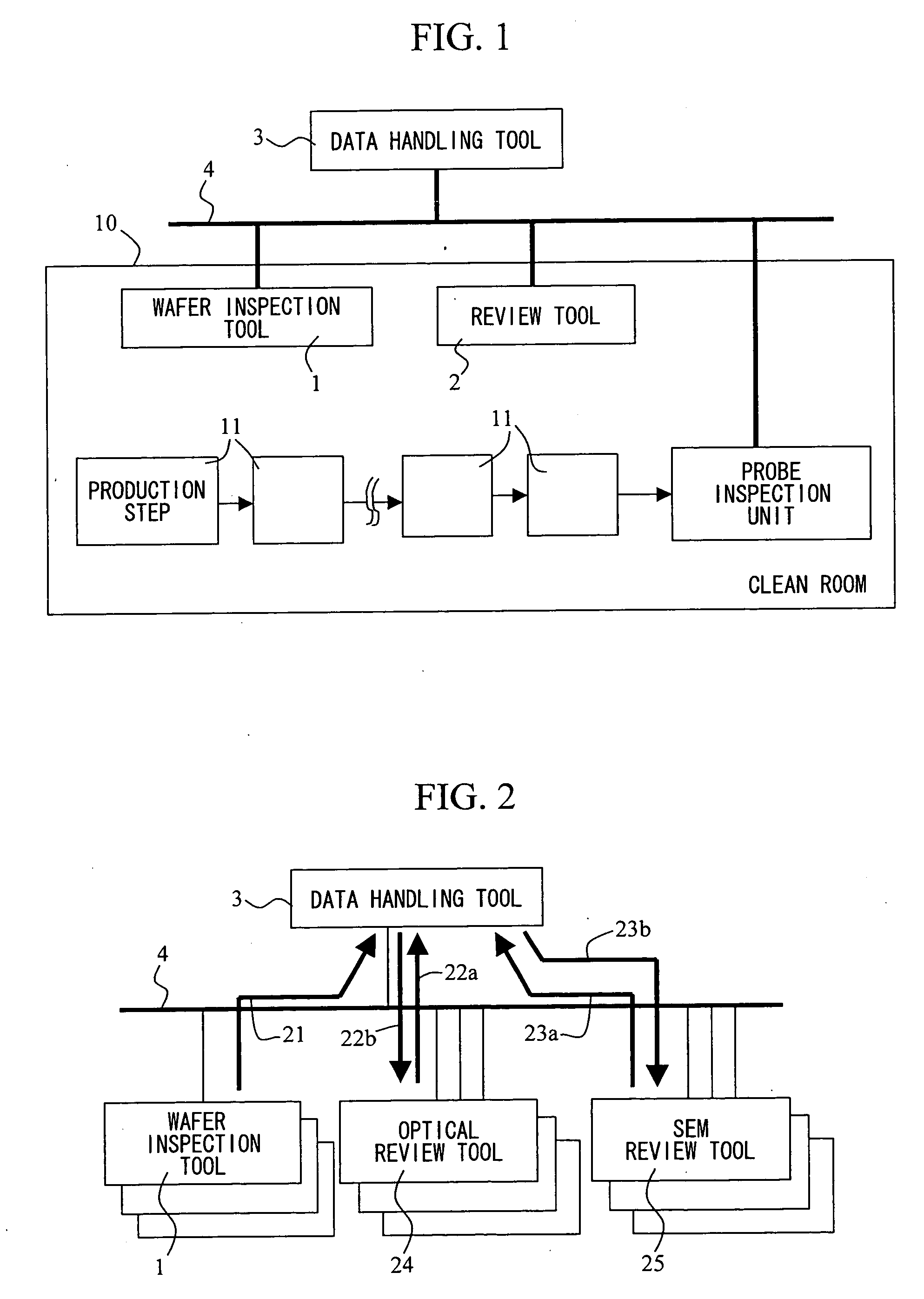
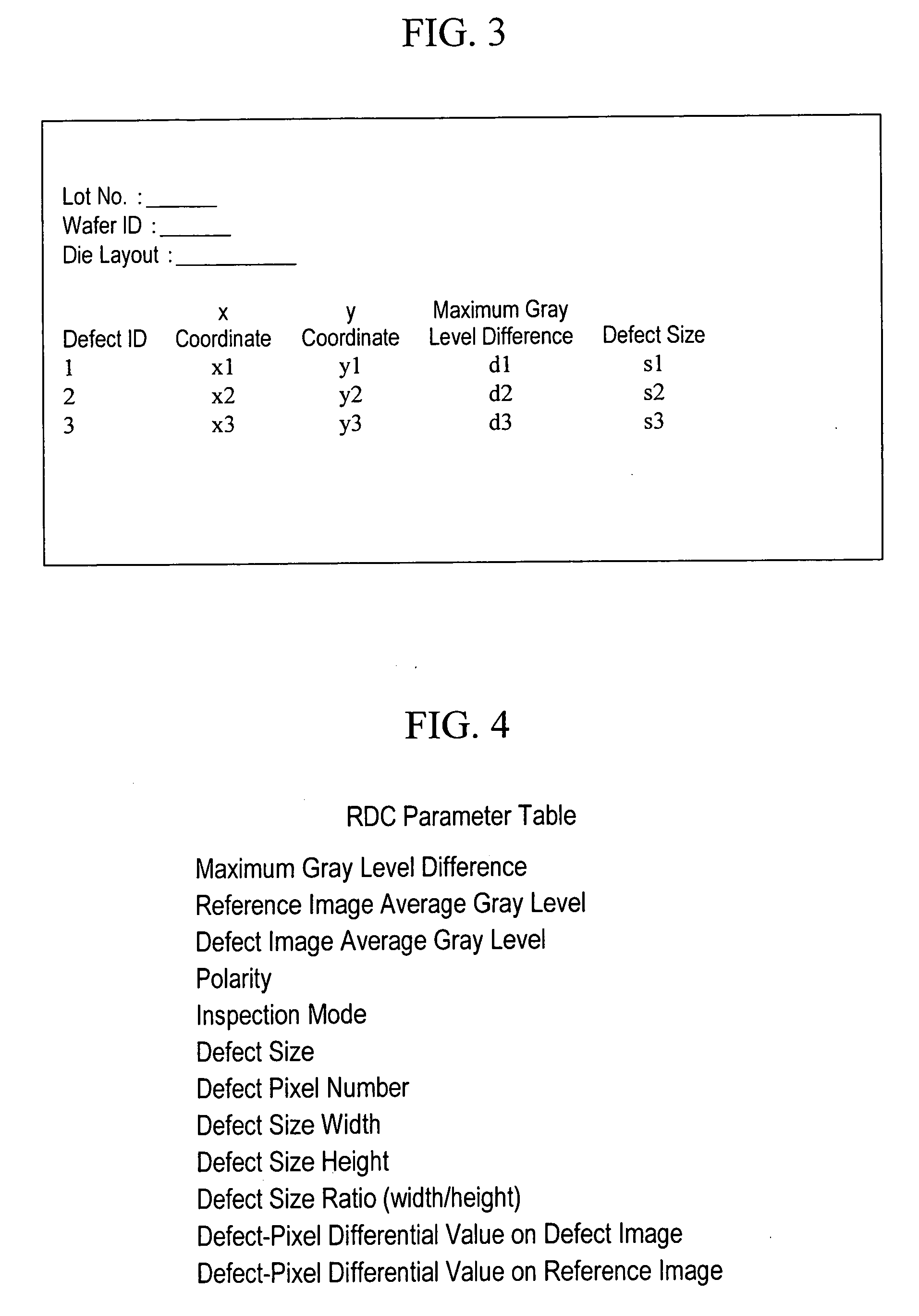
[0030] An example of the defect review assist system of the invention will be described with reference to FIGS. 1, 2, and 3. FIG. 1 shows an example of the overall structure of the system. FIG. 2 shows how the defect attributes and ADR image information provided by the wafer inspection tool and the ADR / ADC information provided by the defect review tool are exchanged. FIG. 3 shows an example of the defect information exchanged between the wafer inspection tool and the defect review tool. While in the example shown in FIGS. 1 and 2 the data handling tool is shown independently provided, alternatively the data handling tool may be integrally constructed with the wafer inspection tool or the defect review tool.

[0031] Semiconductor production steps 11 are normally implemented in a clean room 10 in which a clean envir...


PUM


Abstract

A defect detected by a wafer inspection tool is reliably captured by a defect review tool. A defect review condition in the defect review tool is varied depending on defect attributes provided by the wafer inspection tool so as to optimize the review process. For example, review magnification is varied depending on the size of the defect, or the frame addition number is varied depending on the maximum gray level difference.

Description

CLAIM OF PRIORITY [0001] The present application claims priority from Japanese application JP 2005-326123 filed on Nov. 10, 2005, the content of which is hereby incorporated by reference into this application. BACKGROUND OF THE INVENTION [0002] 1. Field of the Invention [0003] The invention relates to a defect review operation concerning products or components being manufactured. Particularly, the invention relates to a system for improving the efficiency of the process of determining conditions in a tool for detecting particles or pattern defects on the surface of a semiconductor wafer, photo mask, magnetic disc, or liquid crystal display substrate, for example. [0004] 2. Background Art [0005] In semiconductor production, particles or pattern defects on the surface of a wafer during the production process may lead to defective products. Therefore, it is necessary to quantify such particles or pattern defects (to be hereafter referred to as defects) and constantly monitor the manufa...

Claims


Application Information

Patent Timeline
Patent Type & Authority Applications(United States)
IPC IPC(8): H01L21/66
CPCG01N21/8851G01N21/9501G01N2021/8861G03F1/84G03F7/7065
Inventor FUNAKOSHI, TOMOHIROKONISHI, JUNKOKARIYA, YUKOTAKAHASHI, NORITSUGUENDO, FUMIAKI
Owner HITACHI HIGH-TECH CORP
Why Eureka
Try Eureka