
Low-temperature polysilicon display and method for fabricating same

a technology of polysilicon and display panel, which is applied in the field of low-temperature polysilicon display panel and the method of fabricating same, can solve the problems of reducing the throughput of the product, affecting the performance of tfts, and poor performance of tft using rta poly-si, and achieves the effect of higher electron mobility

Active Publication Date: 2007-05-10
OPTRONIC SCI LLC
View PDF10 Cites 5 Cited by
  • Summary
  • Abstract
  • Description
  • Claims
  • Application Information

AI Technical Summary

Benefits of technology

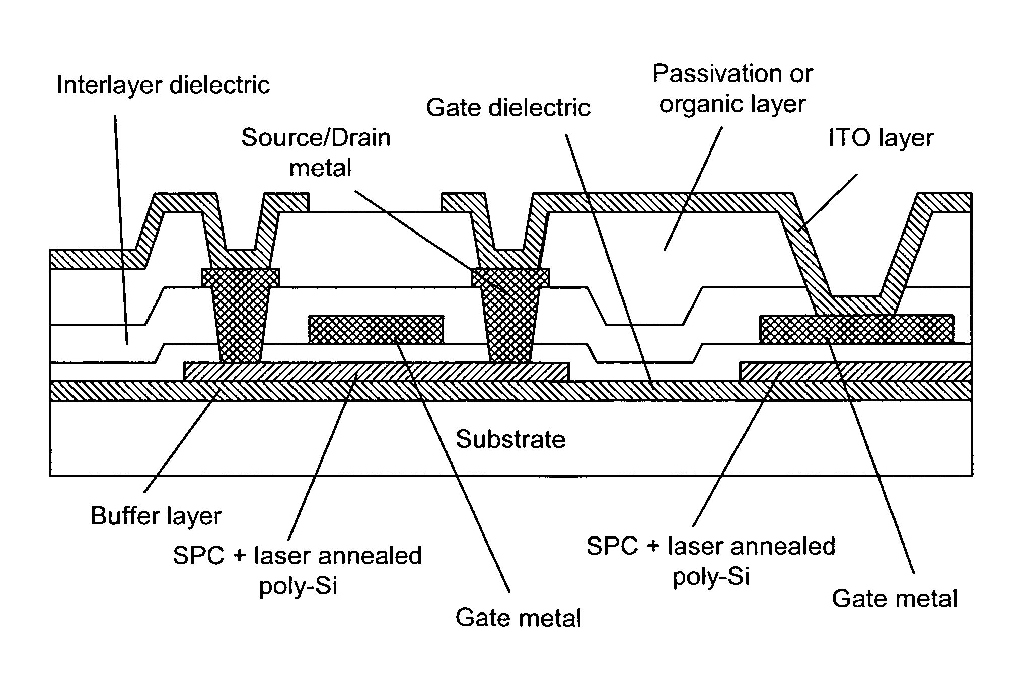
[0004] The present invention provides a method for producing a display panel on a substrate using LTPS technologies. The display panel comprises at least one display area and one peripheral circuit area having electronic components for driving the display components in the display area. In particular, the electronic components in the display area are fabricated substantially on a polysilicon (poly-Si) layer converted from amorphous silicon by a solid phase crystallization (SPC) process, whereas the electronic components in the peripheral circuit area are fabricated substantially on a polysilicon layer converted from amorphous silicon first by the SPC process and then by laser annealing. As such, display area has a more uniform poly-Si layer substantially free of defects associated with laser annealing, and the peripheral circuit has a poly-Si layer with higher electron mobility.

Problems solved by technology

SPC using low-temperature furnace annealing requires very long anneal times and thus reduces the throughput of the product.
Furthermore, crystalline defects detrimentally effect the performance of TFTs.
While rapid thermal annealing (RTA) can increase the throughput, the performance of the TFT using RTA poly-Si is poorer than low-temperature crystallization.
However, due to the instability if the laser beam, the poly-Si area so produced usually has perceptible non-uniformity known as laser mura.
For this reason, poly-Si produced by laser annealing is generally not suitable for high-quality display panels.

Method used


Image

  • Low-temperature polysilicon display and method for fabricating same
  • Low-temperature polysilicon display and method for fabricating same
  • Low-temperature polysilicon display and method for fabricating same

Examples


Embodiment Construction

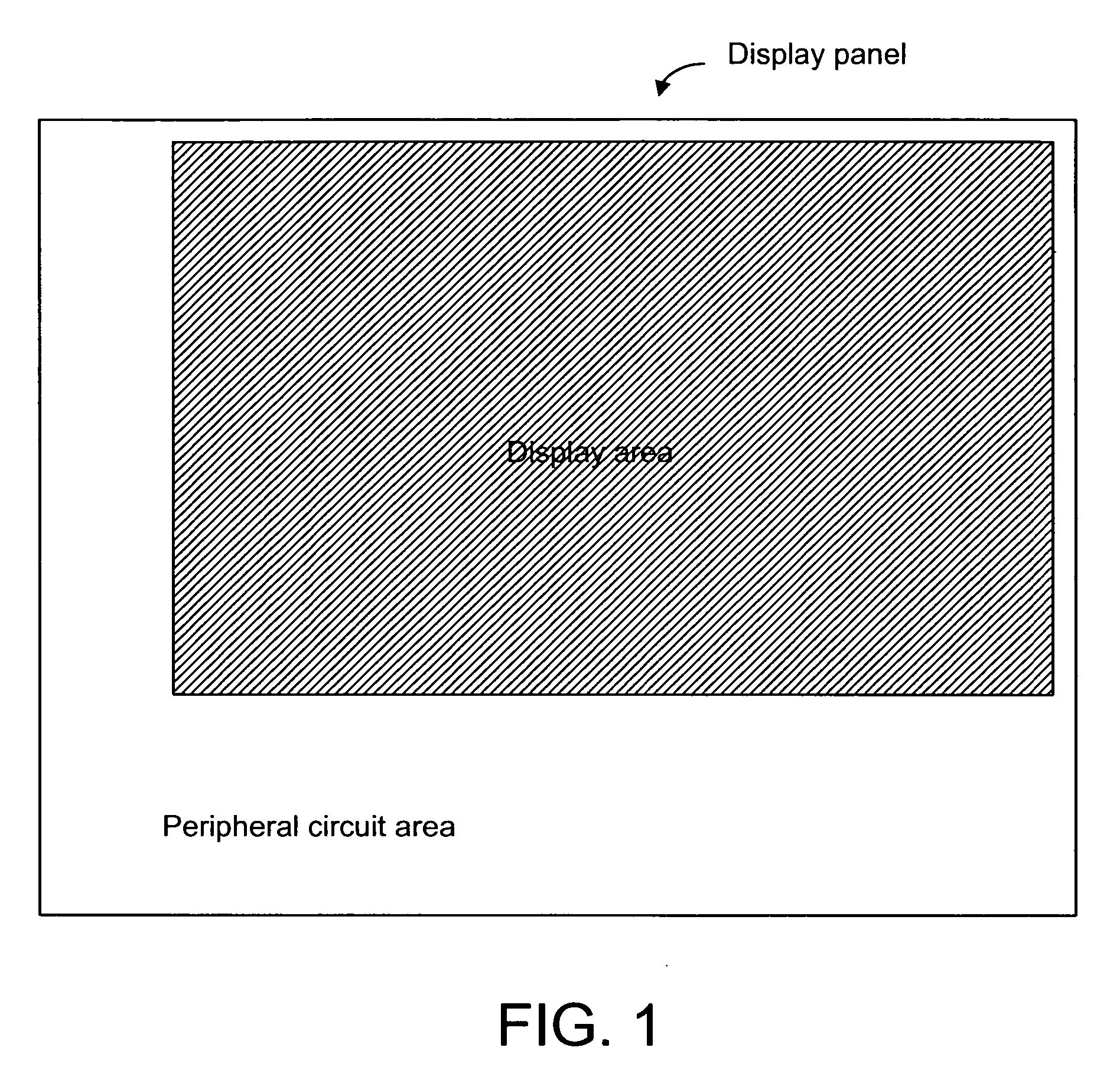
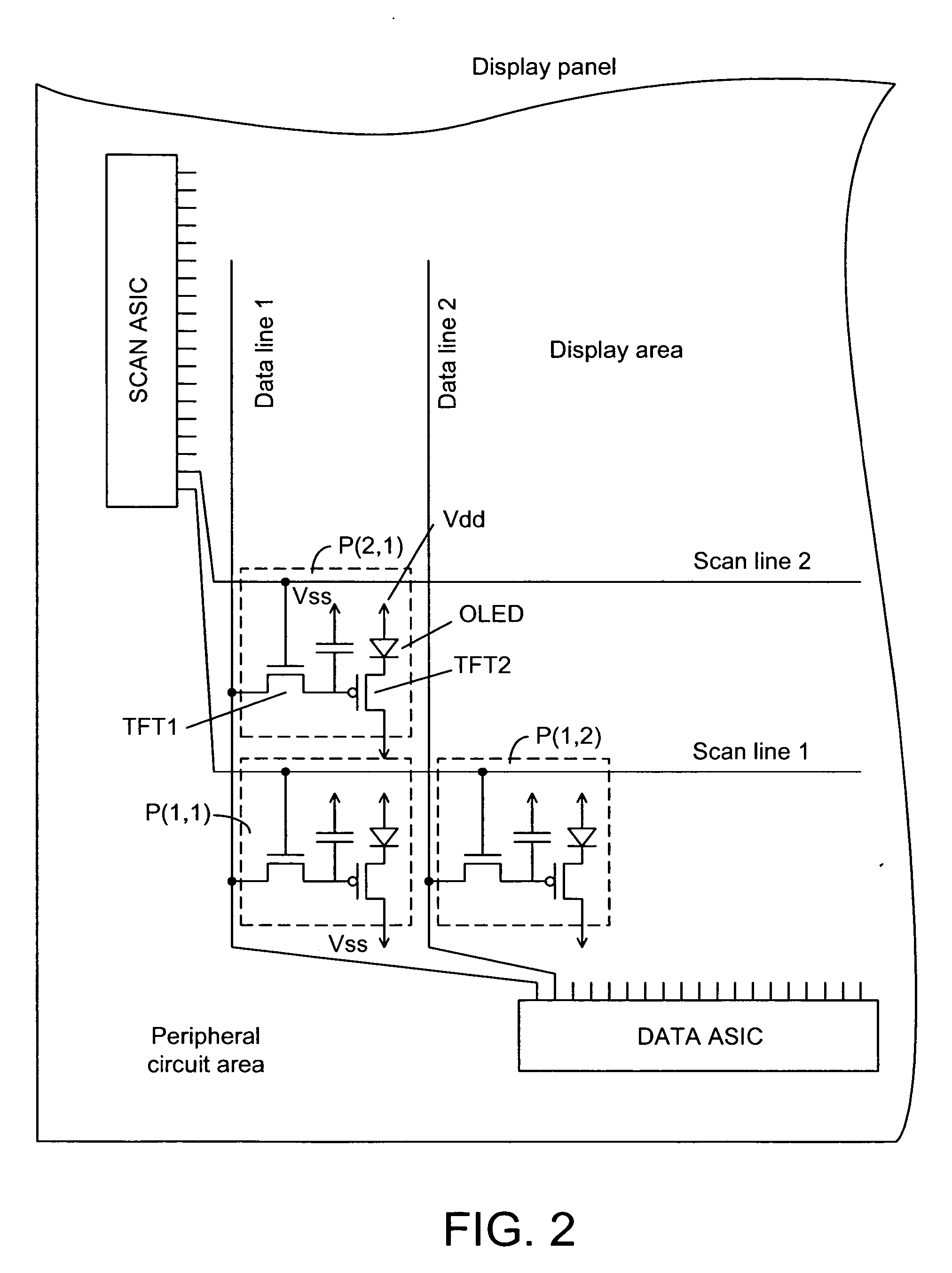
[0012] The present invention uses two different low-temperature polysicon (LTPS) processes to produce a first polysilicon (poly-Si) area and a second poly-Si area on a substrate. The first poly-Si area is mainly used for a display area of a display panel and the second poly-Si area is mainly used for a peripheral circuit area, as shown in FIG. 1. For example, the display panel is an active matrix organic light-emitting diode (AMOLED) panel. The display area comprises a plurality of AMOLED pixels arranged in a two-dimensional array. The peripheral circuit area in the display panel includes a plurality of integrated circuits and bus-lines or connectors to provide data and control signals to the pixels. As shown in FIG. 2, the integrated circuits in the peripheral circuit area include one or more DATA ASICs and one or more SCAN ASICs. The display area comprises a row of pixel (1,1), pixel (1,2), . . . that share a Scan line from the SCAN ASIC, and a column of pixel (1,1), pixel (2,1) ....


PUM


Abstract

A display panel comprising at least one display area and one peripheral circuit area having electronic components for driving the display components in the display area. The electronic components in the display area are fabricated substantially on a polysilicon layer converted from amorphous silicon by a solid phase crystallization process, whereas the electronic components in the peripheral circuit area are fabricated substantially on a polysilicon layer converted from amorphous silicon first by the solid phase crystallization process and then by laser annealing. As such, display area has a more uniform poly-Si layer substantially free of defects associated with laser annealing, and the peripheral circuit has a poly-Si layer with higher electron mobility.

Description

FIELD OF THE INVENTION [0001] The present invention relates generally to a display panel having a display area and an electronic circuit area and, more particularly, to a display panel made substantially of low-temperature polysilicon. BACKGROUND OF THE INVENTION [0002] Polysilicon (poly-Si) thin-film transistors (TFTs) have been used in a flat-panel display such as an active matrix liquid crystal display (AMLCD) panel. The channel films for this type of display are typically deposited in the amorphous phase and then crystallized to form smooth, large grain polysilicon. In particular, solid-phase crystallization (SPC) is a promising technique for converting amorphous silicon (a-Si) into polysilicon. The crystallization from an amorphous phase to a poly-crystalline phase occurs through a nucleation process and a grain growth process. In a SPC Si system, it is desirable to achieve the largest possible grains, and therefore, it is desirable to suppress nucleation relative to grain grow...

Claims


Application Information

Patent Timeline
IPC IPC(8): H01L21/84H01L31/113
CPCG02F1/13454H01L27/1285H01L27/1296H01L27/3244H10K59/12
Inventor PENG, CHIA-TIEN
Owner OPTRONIC SCI LLC
Learn More