Oxygen depleted etching process

a technology of oxygen depletion and etching process, which is applied in the manufacture of basic electric elements, semiconductor/solid-state devices, electric devices, etc., can solve the problems of high-temperature plasma etching process exceeding the thermal budget of photoresist materials, limited use of photoresist as hard masks, and yield reducing defects in devices

Inactive Publication Date: 2007-05-10
UNITY SEMICON
View PDF3 Cites 120 Cited by
  • Summary
  • Abstract
  • Description
  • Claims
  • Application Information

AI Technical Summary

Problems solved by technology

Although conventional photoresist materials can be used as a mask layer, high temperature plasma etching processes can exceed a thermal budget of photoresist materials.
Consequently, the use of photoresist as a hard mask is limited to low temperature plasma etching processes where the processing temperatures is less than approximately 150° C.
Eventually, when the plasma etching process terminates, the residue can remain on a bottom most layer and that residue can result in a yield reducing defect in a device.
The residue 115r can cause defects or contamination that can reduce device yields.

Method used


Image

  • Oxygen depleted etching process
  • Oxygen depleted etching process
  • Oxygen depleted etching process

Examples


first embodiment

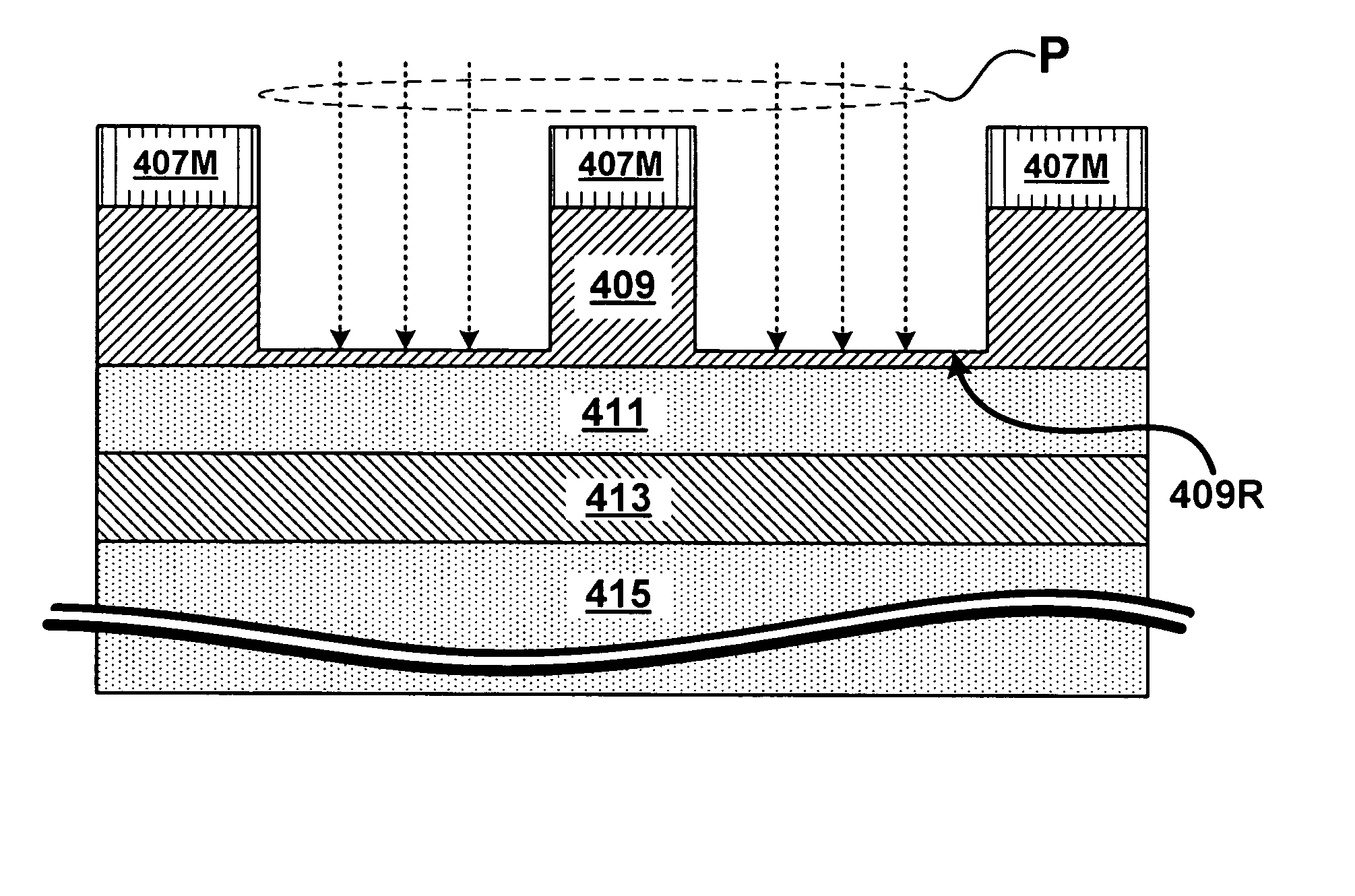
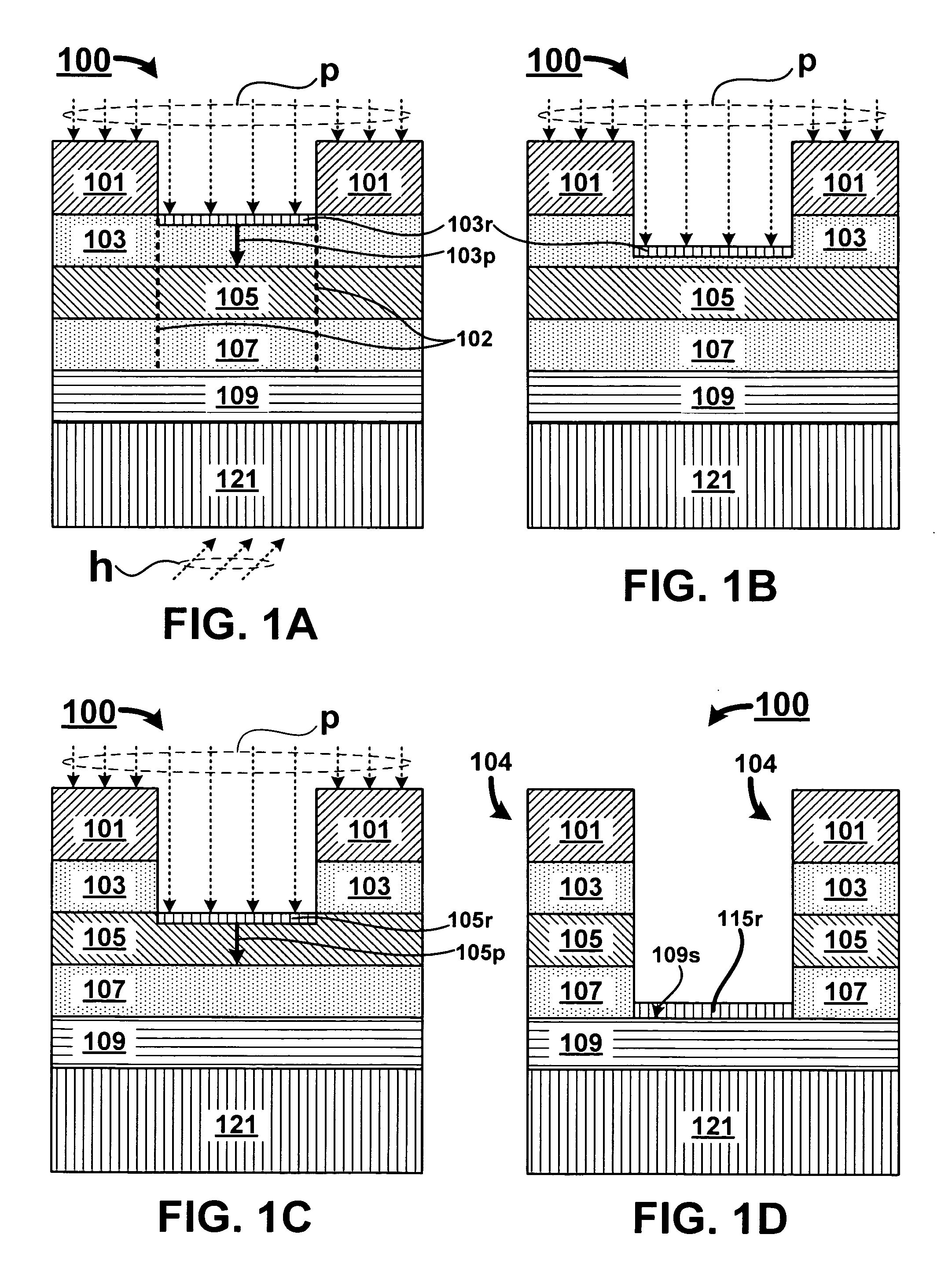
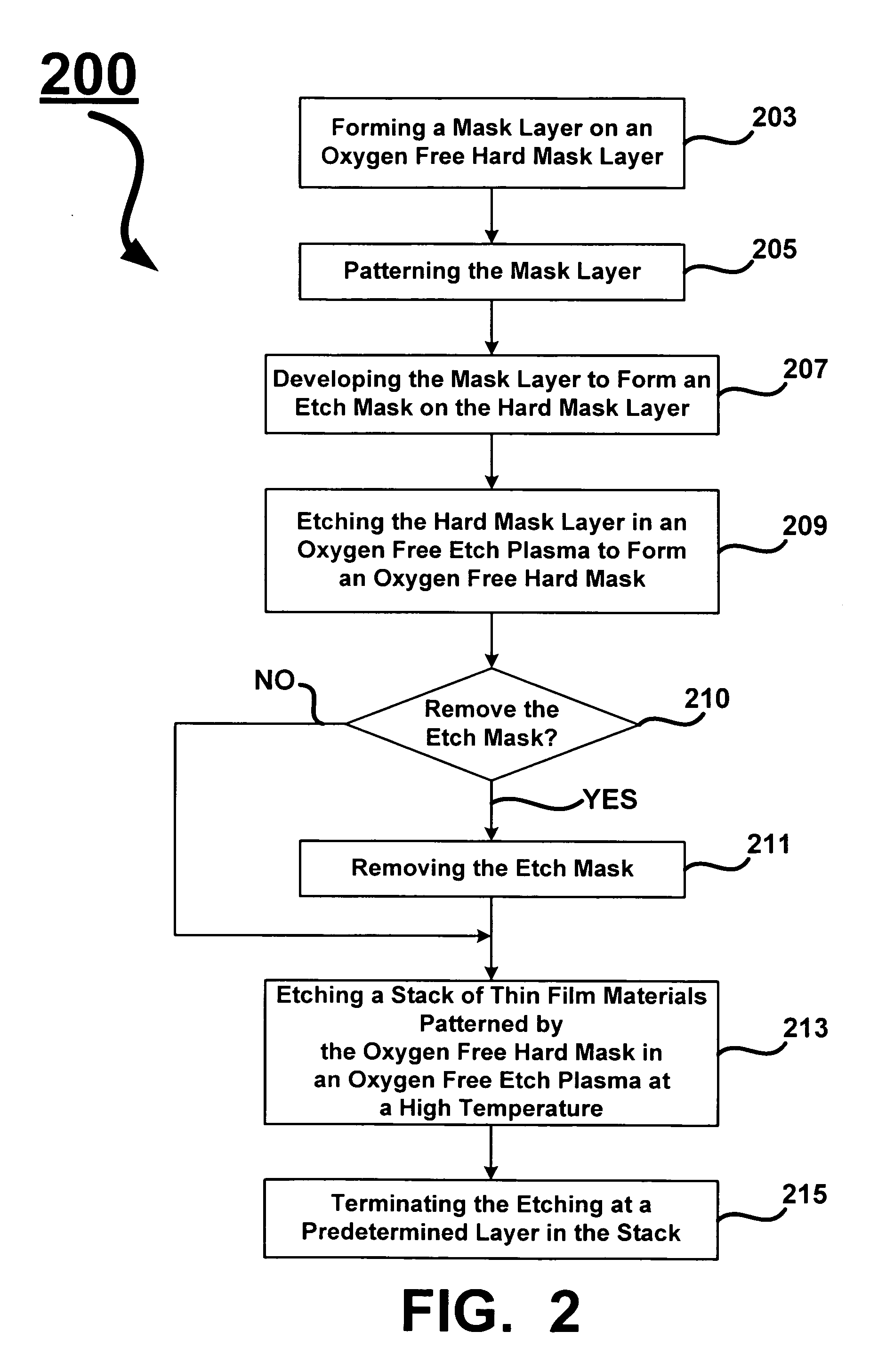
[0036] As shown in the drawings for purpose of illustration, the present invention is embodied in a method of oxygen depleted etching of thin films at a high temperature. In a first embodiment, the method includes forming a mask layer on an oxygen free hard mask layer, patterning the mask layer, developing the mask layer to form an etch mask on the oxygen free hard mask layer, etching the oxygen free hard mask layer in an oxygen free etch plasma to form an oxygen free hard mask, optionally removing the etch mask, etching a stack of thin film materials patterned by the oxygen free hard mask in an oxygen free etch plasma at a high temperature, and terminating the etching at a predetermined layer in the stack of thin film materials.

second embodiment

[0037] In a second embodiment, the method includes forming a mask layer on a hard mask layer that is not oxygen free, patterning the mask layer, developing the mask layer to form an etch mask on the hard mask layer, etching the hard mask layer in a substantially oxygen free etch plasma to form a hard mask, optionally removing the etch mask, etching a stack of thin film materials patterned by the hard mask in a substantially oxygen free etch plasma at a high temperature, and terminating the etching at a predetermined layer in the stack of thin film materials.

third embodiment

[0038] In a third embodiment, the method includes forming a mask layer on an oxygen free titanium hard mask layer, patterning the mask layer, developing the mask layer to form an etch mask on the oxygen free titanium hard mask layer, etching the oxygen free titanium hard mask layer in an oxygen free etch plasma to form an oxygen free titanium hard mask, etching a stack of thin film materials patterned by the oxygen free titanium hard mask in an oxygen free etch plasma at a high temperature, and terminating the etching at a predetermined layer in the stack of thin film materials.


PUM

PropertyMeasurementUnit
temperatureaaaaaaaaaa
temperaturesaaaaaaaaaa

Abstract

A method for oxygen depleted plasma etching and mixed mode plasma etching are disclosed. The method includes using an oxygen free etch plasma or a substantially oxygen free etch plasma at a high temperature to etch a stack including a plurality of layers of thin film materials. The oxygen depleted etching prevents or substantially reduces by-product re-deposition of titanium oxides generated by etching of titanium thin films in the stack. The titanium oxides can serve as a secondary mask layer that can cause defects in devices formed from the stack. Mixed mode plasma etching can include etching the stack with an oxygen free plasma, a substantially oxygen free plasma, and an oxygen containing plasma at different stages of a process.

Description

FIELD OF THE INVENTION [0001] The present invention relates generally to processing of thin film structures. More specifically, the present invention relates to plasma etching processes for etching thin film structures. BACKGROUND OF THE INVENTION [0002] Titanium (Ti), titanium oxide (TiO), and titanium nitride (TiN) thin films have been used as glue layers (also called adhesion layers) and barrier layers in semiconductor and microelectronic applications. Titanium (Ti) and titanium nitride (TiN) can also be used as hard mask layers for various etching steps due to their resilient etch characteristics, particularly at high etch temperatures encountered in dry etching (e.g., plasma etching) processes. Although conventional photoresist materials can be used as a mask layer, high temperature plasma etching processes can exceed a thermal budget of photoresist materials. At processing temperatures that rise above approximately 150° C., photoresist will begin to reticulate. As the processi...

Claims


Application Information

Patent Timeline
Patent Type & Authority Applications(United States)
IPC IPC(8): H01L21/465
CPCH01L21/31116H01L21/32136H01L21/32139
Inventor OH, TRAVIS BYONGHYOP
Owner UNITY SEMICON
Why Eureka
Try Eureka