Method for forming patterns and thin film transistors
a thin film transistor and pattern technology, applied in the field of pattern formation, can solve the problems of poor adhesion between the film and the substrate, thermal expansion coefficient, and substrate warpage, and achieve the effect of reducing the stress of the film efficiently and improving the yield rate of the thin film transistor
- Summary
- Abstract
- Description
- Claims
- Application Information
AI Technical Summary
Benefits of technology
Problems solved by technology
Method used
Image

Examples
first embodiment
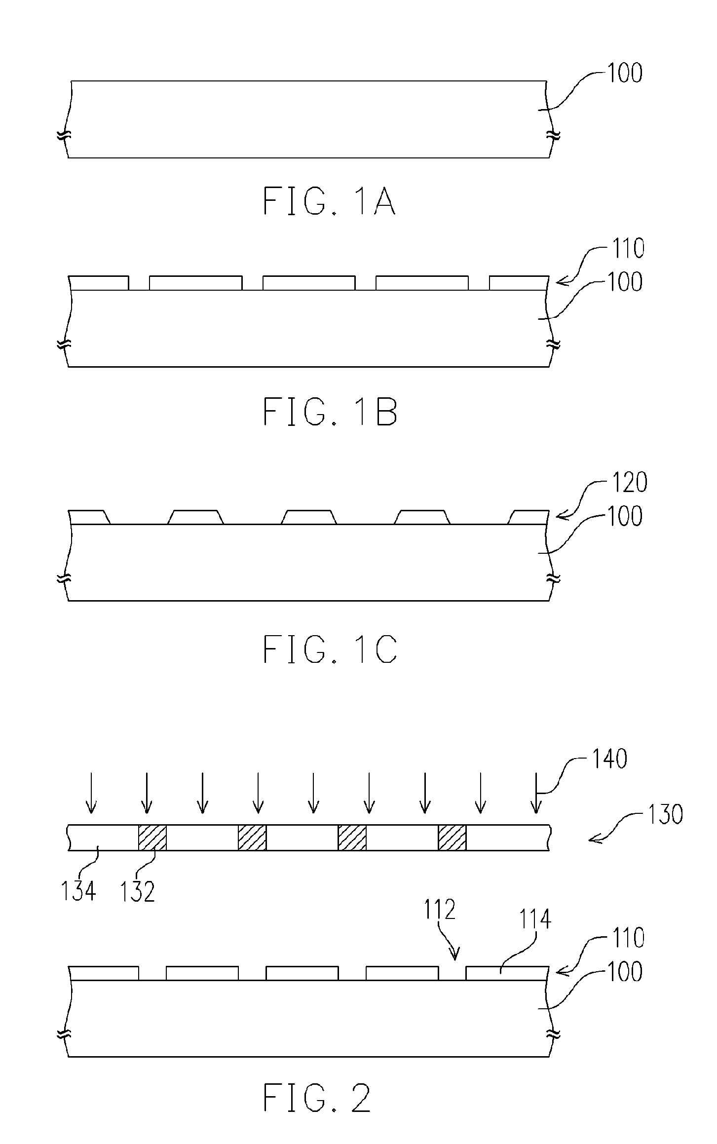
[0038]FIGS. 1A to 1C are schematic, cross-sectional diagrams illustrating the process flow for forming a pattern according to a preferred embodiment of the present invention. First, please refer to FIG. 1A, a substrate 100 is provided. Next, please refer to FIG. 1B, a discontinuous film 110 is formed on the substrate 100 to reduce the stress of the film 110. Finally, please refer to FIG. 1C, the discontinuous film 110 is patterned to form a pattern 120.
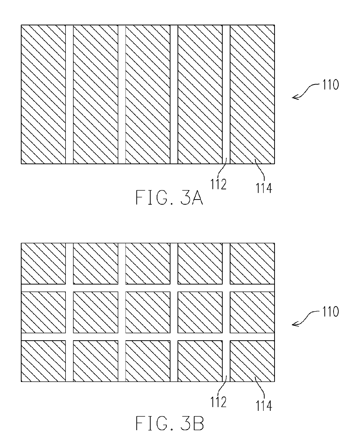
[0039] In an embodiment of the present invention, the method for forming the discontinuous film 110 on the substrate 100 as shown in FIG. 1B comprises a step of performing a deposition process 140 (shown in FIG. 2) by using a shadow mask 130. The deposition process 140 can be a chemical vapor deposition (CVD) process or a physical vapor deposition (PVD) process.
[0040]FIG. 2 is a schematic side view showing that a deposition process is performed by using a shadow mask according to a preferred embodiment of the present invention. Plea...
second embodiment
[0047] The method for forming a pattern of the first embodiment can be applied to the fabrication process of a thin film transistor of the second embodiment. The thin film transistor can be a low temperature poly silicon thin film transistor (LTPS TFT) for example. FIGS. 6A to 6G are schematic, cross-sectional diagrams illustrating the process flow for making a thin film transistor according to a preferred embodiment of the present invention.
[0048] First, please refer to FIG. 6A, a substrate 300 is provided. The substrate 300 can be a glass substrate, a silicon substrate or a flexible substrate for example.
[0049] Next, a poly silicon island 340 is formed on the substrate 300 (as shown in FIG. 6D). In an embodiment of the present invention, the method of forming the poly silicon island 340 is shown in FIGS. 6B to 6D for example. Please refer to FIG. 6B, an amorphous silicon layer 320 is formed on the substrate 300 while the amorphous silicon layer 320 is a discontinuous film. Next,...
third embodiment
[0060]FIGS. 9A to 9E are schematic, cross-sectional diagrams illustrating the process flow for forming a thin film transistor according to another embodiment of the present invention.
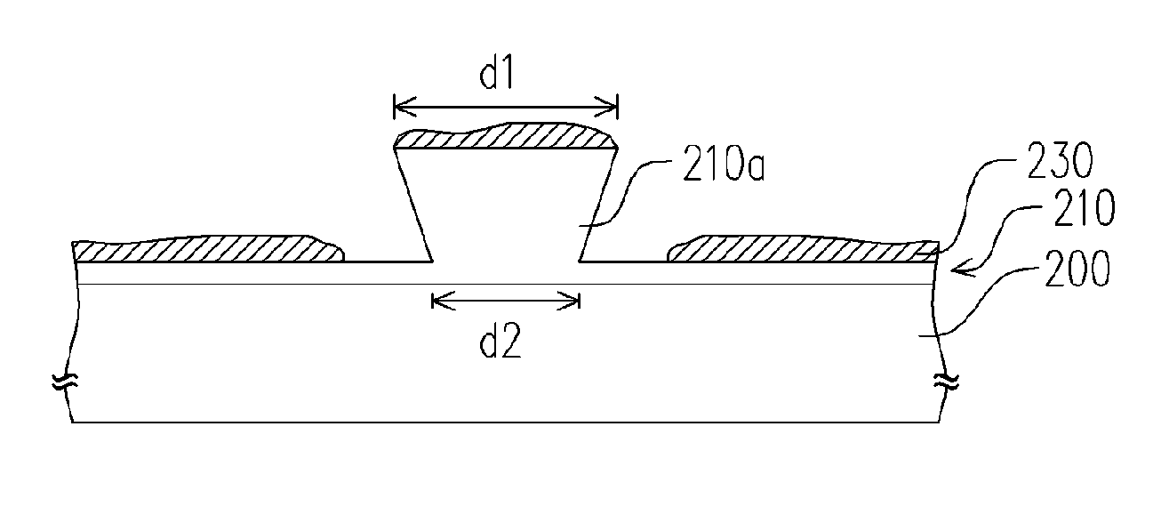
[0061] First, please refer to FIG. 9A, a gate 510 is formed on a substrate 500. Next, please refer to FIG. 9B, a gate insulating layer 520 is formed on the substrate 500 to cover the gate 510. After that, please refer to FIG. 9C, a channel layer 530 is formed on the gate insulating layer 520 and the gate 510. Thereafter, please refer to FIG. 9D, a source / drain 550 is formed on the channel layer 530. At least one of the gate 510, the channel layer 530 and the source / drain 550 is formed by using the method for forming a pattern disclosed in the first embodiment.
[0062] Next, please refer to FIG. 9C, in an embodiment of the present invention, before the source / drain 550 is formed, the method further comprises a step of forming an ohmic contact layer 540 on the channel layer 530 for example. The ohmic cont...
PUM
| Property | Measurement | Unit |
|---|---|---|
| stress | aaaaa | aaaaa |
| insulating | aaaaa | aaaaa |
| thermal expansion coefficient | aaaaa | aaaaa |
Abstract
Description
Claims
Application Information
 - R&D
- Intellectual Property
- Life Sciences
- Materials
- Tech Scout
- Unparalleled Data Quality
- Higher Quality Content
- 60% Fewer Hallucinations
Browse by: Latest US Patents, China's latest patents, Technical Efficacy Thesaurus, Application Domain, Technology Topic, Popular Technical Reports.
© 2025 PatSnap. All rights reserved.Legal|Privacy policy|Modern Slavery Act Transparency Statement|Sitemap|About US| Contact US: help@patsnap.com