Sputtering target and method for finishing surface of such target
- Summary
- Abstract
- Description
- Claims
- Application Information
AI Technical Summary
Benefits of technology
Problems solved by technology
Method used
Image
Examples
example 1
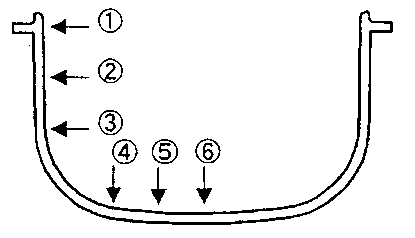
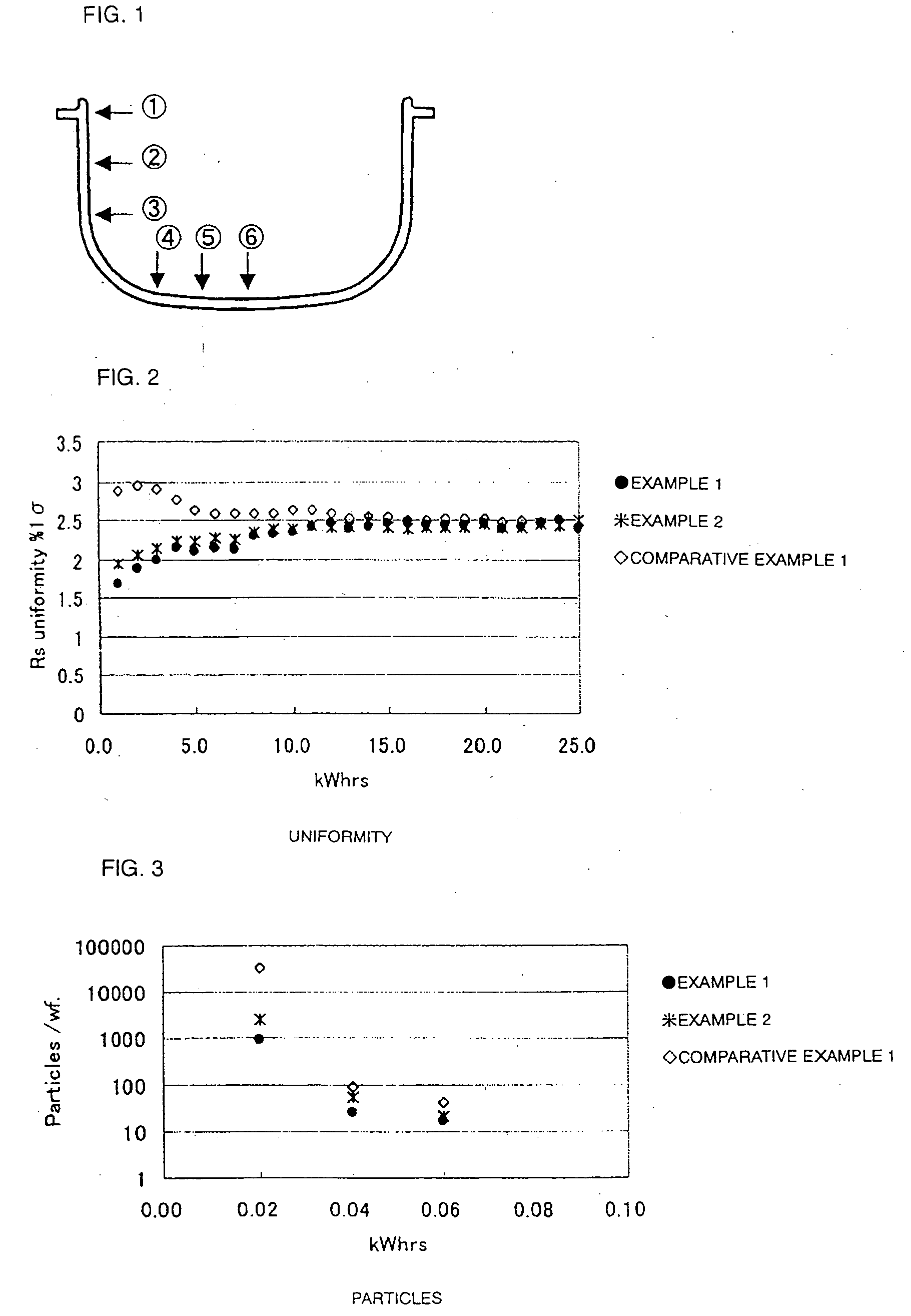
[0031] The inside face of a Ti hollow cathode target was finished by being subject to lathe processing, polishing (sandpapering) and etching. The outline of the obtained hollow cathode sputtering target is shown in FIG. 1. The measurement of the surface roughness of the target was conducted at the respective measurement points (1 to 6) shown in FIG. 1.
[0032] Table 1 shows the surface roughness Ra (μm) of the inside of the target. As shown in Table 1, the surface roughness Ra of the bottom face corresponding to the measurement points 1 to 6 is 0.5% m or less, and the surface roughness Ra of the cylindrical inner peripheral face was also 0.5 μm or less.
[0033] The results upon performing a sputtering test with this hollow cathode target are shown in FIG. 2 and FIG. 3. The uniformity showed favorable values from the initial stage, and there were roughly 900 particles on a single wafer. Further, peeling of the redeposited film of the inner bottom could not be observed up to the expecte...
example 2
[0034] The inside face of a Ti hollow cathode target was finished by being subject to lathe processing, polishing (sandpapering) and etching so as to be Ra (μm)<1.0.
[0035] As with Example 1, the measurement of the surface roughness of the target was conducted at the respective measurement points (1 to 6) shown in FIG. 1. The results are similarly shown in Table 1.
[0036] As shown in Table 1, the surface roughness Ra of the bottom face corresponding to the measurement points 1 to 6 is 1.0 μm or less, and the surface roughness Ra of the cylindrical inner peripheral face was also 1.0 μm or less.
[0037] The results upon performing a sputtering test with this hollow cathode target are shown in FIG. 2 and FIG. 3. As shown in FIG. 2, the uniformity showed favorable values from the initial stage. Also, as shown in FIG. 3, there were roughly 2,500 particles on a single wafer. Further, peeling of the redeposited film at the bottom of the inside face could not be observed up to the expected u...
example 3
[0042] The inside face of a Ta hollow cathode target was finished by being subject to lathe processing, polishing (sandpapering) and etching. As with Example 1, the measurement of the surface roughness of the target was conducted at the respective measurement points (1 to 6) shown in FIG. 1.
[0043] The surface roughness Ra (μm) of the inside face of the target is shown in Table 1. As shown in Table 1, the surface roughness Ra at the measurement points 1 to 6 was 0.4 to 0.5 μm.
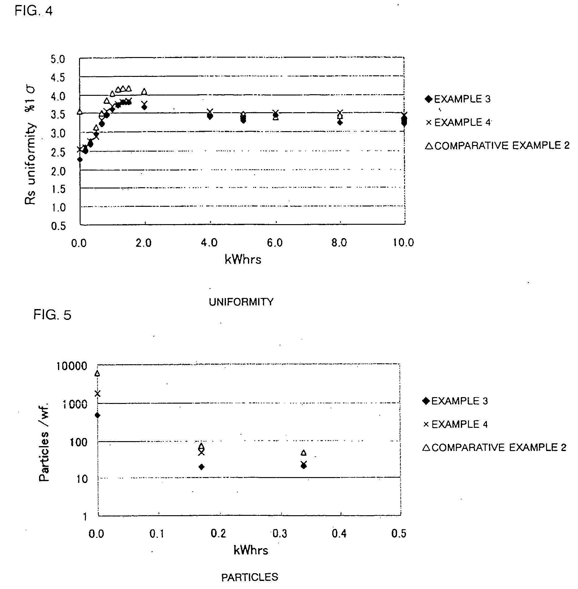
[0044] As a result of performing a sputtering test with this hollow cathode target, as shown in FIG. 4, the uniformity showed favorable values from the initial stage. Also, as shown in FIG. 5, there were roughly 500 particles on a single wafer. Further, peeling of the redeposited film at the bottom of the inside face could not be observed up to the expected useful life.
PUM
| Property | Measurement | Unit |
|---|---|---|
| Surface roughness | aaaaa | aaaaa |
Abstract
Description
Claims
Application Information


