Operation method of non-volatile memory
a non-volatile memory and operation method technology, applied in the field of semiconductor devices, can solve the problems of difficult to completely pattern the oxide/nitride/oxide layer of the sonos memory cell, difficult to achieve the effect of simple structure of the non-volatile memory
- Summary
- Abstract
- Description
- Claims
- Application Information
AI Technical Summary
Benefits of technology
Problems solved by technology
Method used
Image


Examples
Embodiment Construction
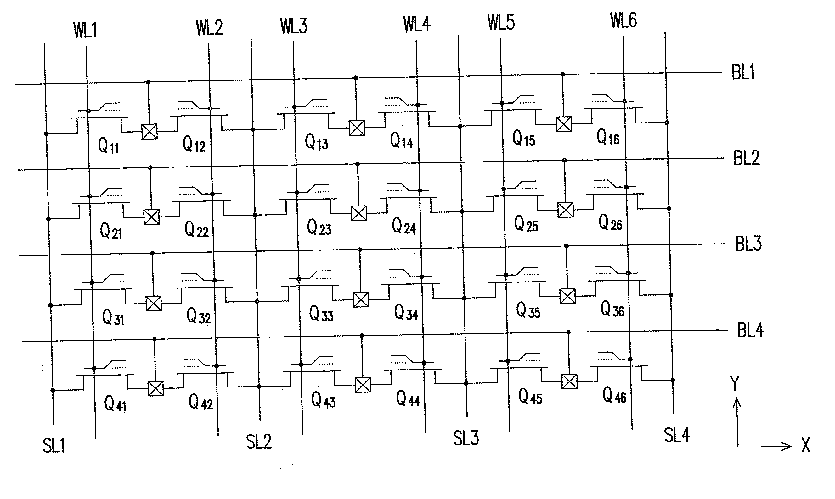
[0053]FIG. 1A is a cross-sectional diagram of a non-volatile memory cell according to an exemplary embodiment of the present invention.
[0054] Referring to FIG. 1A, a memory cell 101a is, for example, formed on a first conductive type substrate 100. The first conductive type substrate 100 is, for example, a silicon substrate. The memory cell is, for example, composed of a gate dielectric layer 102, a gate 104, a dielectric layer 106, charge storage layers 108a and 108b, a second conductive type source region 110, a second conductive type drain region 112, and a second conductive type lightly doped region 114.
[0055] The gate 104 is, for example, formed on the first conductive type substrate 100. The material of the gate 104 is, for example, doped polysilicon.
[0056] The gate dielectric layer 102 is, for example, formed between the gate 104 and the first conductive type substrate 100. The material of the gate dielectric layer 102 is, for example, silicon oxide.
[0057] The second cond...
PUM
 Abstract
Description
Claims
Application Information