Bonding method, device produced by this method, and bonding device

a technology of bonding and a bonding device, which is applied in the manufacture of microstructural devices, microstructured devices, electrical devices, etc., can solve the problems of unavoidable adhesion of organic substances to the surface of wafers and the inability to achieve firm bonding of si (semiconductor), so as to increase the bonding strength and increase the production efficiency

Active Publication Date: 2007-05-17
BONDTECH
View PDF8 Cites 76 Cited by
  • Summary
  • Abstract
  • Description
  • Claims
  • Application Information

AI Technical Summary

Benefits of technology

[0105] An effect of the present invention is that anodic bonding is performed after surface activation using an energy wave, thereby performing bonding at lower temperature and increasing a bonding strength, and also, after performing preliminary bonding due to surface activation, main bonding due to the anodic bonding is perfor

Problems solved by technology

In the conventional technique, the wafers are transported in the atmospheric air, so that organic substances unavoidably adhere to surfaces of the wafers.
In this method, however, organic substances or oxide film is removed from a surface to prepare a surface which is electrically activated with metal dangling bond so that bonding is performed due to

Method used


Image

  • Bonding method, device produced by this method, and bonding device
  • Bonding method, device produced by this method, and bonding device
  • Bonding method, device produced by this method, and bonding device

Examples


Embodiment Construction

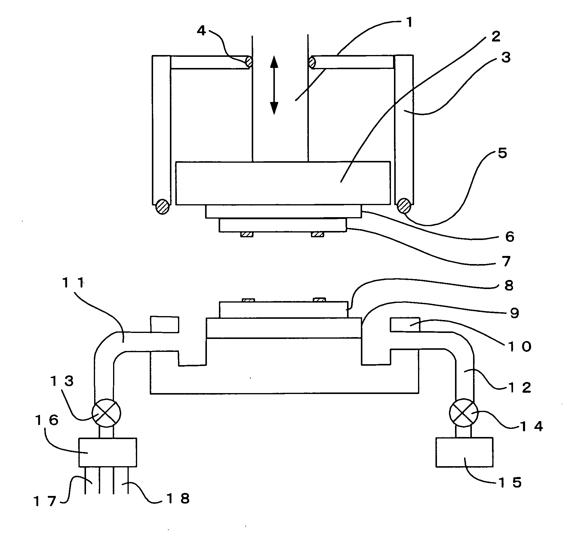
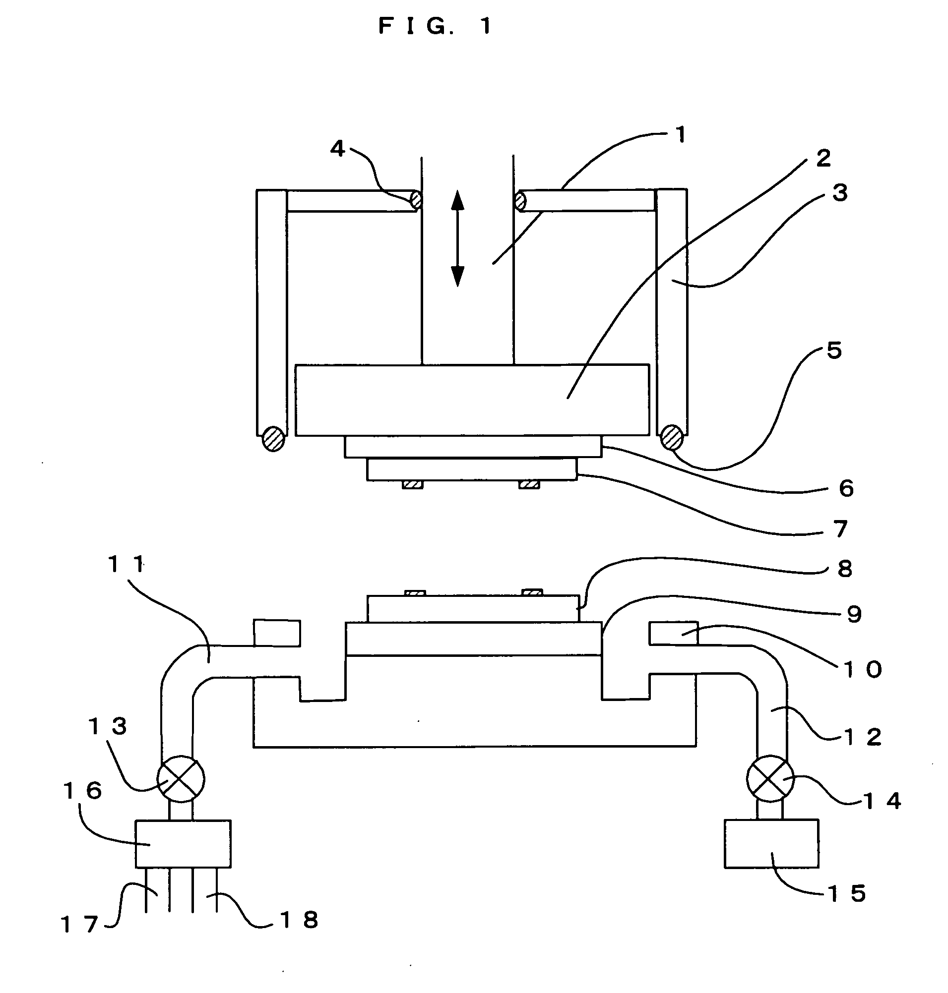
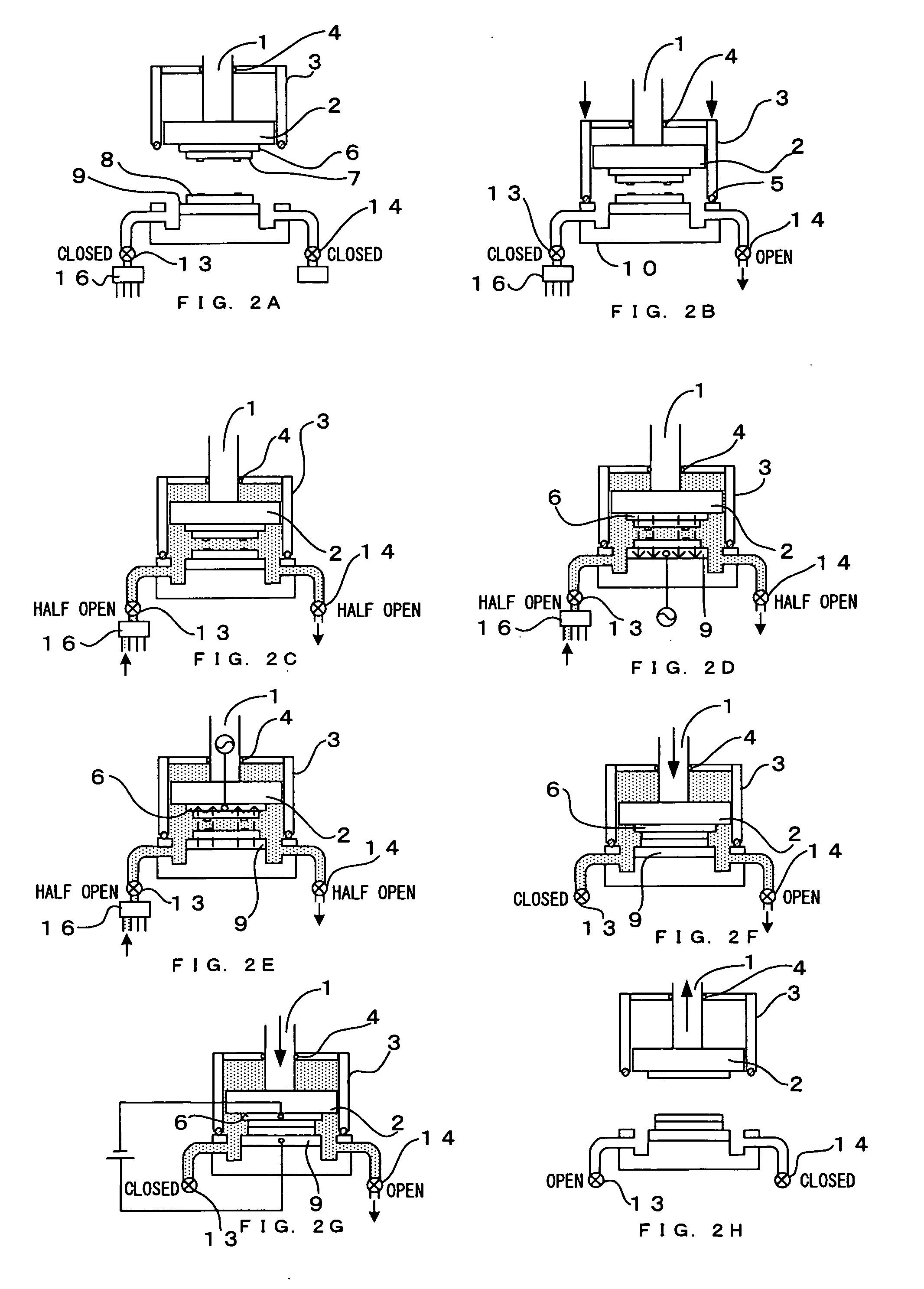
[0175] In this embodiment, a method and a bonding device are provided in which wafers (objects to be bonded) are surface-activated using a plasma, preliminary bonding is performed, and anodic bonding is performed in a separate main bonding step. Hereinafter, a desired embodiment of the present invention will be described with reference to the accompanying drawings. FIG. 7 illustrates a configuration according to an embodiment of the present invention in which preliminary bonding due to surface activation and main bonding due to anodic bonding are separated, thereby increasing production efficiency.

[0176] As illustrated in FIG. 7, bonding surfaces are surface-activated using a plasma treatment device A (energy wave treatment device), room temperature preliminary bonding is performed in a vacuum using a preliminary bonding device B, and main bonding with heating is performed in the atmospheric air using a plurality of main bonding devices C (three in FIG. 7), which are used in balanc...


PUM

PropertyMeasurementUnit
Temperatureaaaaaaaaaa
Nanoscale particle sizeaaaaaaaaaa
Temperatureaaaaaaaaaa

Abstract

Conventional heat bonding and anodic bonding require heating at high temperature and for a long time, leading to poor production efficiency and occurrence of a warp due to a difference in thermal expansion, resulting in a defective device. Such a problem is solved. An upper wafer 7 made of glass and a lower wafer 8 made of Si are surface-activated using an energy wave before performing anodic bonding, thereby performing bonding at low temperature and increasing a bonding strength. In addition, preliminary bonding due to surface activation is performed before main bonding due to anodic bonding is performed in a separate step or device, thereby increasing production efficiency, and enabling bonding of a three-layer structure without occurrence of a warp.

Description

TECHNICAL FIELD [0001] The present invention relates to a technique of attaching a plurality of objects to be bonded (wafers, etc.) together by anodic bonding. BACKGROUND ART [0002] Conventionally, there is a known method for bonding a wafer made of Si and a wafer made of glass together by applying a voltage using a electrode for the glass wafer as a cathode while both the wafers are contacted with each other and heating to as high as about 400° C. to 500° C. (anodic bonding). In the conventional technique, the wafers are transported in the atmospheric air, so that organic substances unavoidably adhere to surfaces of the wafers. The strength is as weak as 3 MPa at 200° C. as illustrated in FIG. 5, and therefore, the strength is increased to about 9 MPa by heating at a high temperature of about 400° C. In other words, conventional anodic bonding requires high-temperature heating as well. [0003] Patent Document 1 discloses an exemplary room-temperature bonding method of etching metals...

Claims


Application Information

Patent Timeline
IPC IPC(8): H01L21/30C03C23/00C03C27/00C03C27/02C03C27/06H01L21/00H01L21/762
CPCB81C3/001B81C2201/019C03C23/0005C03C27/00C03C27/06H01L21/67092H01L21/76251
Inventor OKADA, MASUAKI
Owner BONDTECH
Why Eureka
Try Eureka