Beam dose computing method and writing method and record carrier body and writing apparatus

a computing method and beam dose technology, applied in the field of beam dose computing method and writing method, can solve the problems of reducing the accuracy of ultrafine circuit pattern being written, affecting the accuracy of ultrafine circuit pattern writing, and remaining very difficult for the existing technology to completely preven

Active Publication Date: 2007-05-24
NUFLARE TECH INC
View PDF2 Cites 70 Cited by
  • Summary
  • Abstract
  • Description
  • Claims
  • Application Information

AI Technical Summary

Problems solved by technology

Unfortunately, it remains very difficult for the existing technology to completely prevent any undesired variations or fluctuations of line pattern sizes.
This proximity effect-raised size variations would result in a decrease in accuracy of ultrafine depiction pattern having downscaled minimum feature sizes.
A further size variation risk that can lower the accuracy of ultrafine circuit pattern being written is the phenomenon known as “fogging” effect among technicians in the semiconductor lithography art.
One of the currently challenged approaches is to perform size-different variation correction processing tasks with respect to “global” and “local” divided regions of a target mask.
The fog effect correction is based on the per-region relative dose, so pattern line-width variations occurring due to the loading effect are hardly correctable.

Method used


Image

  • Beam dose computing method and writing method and record carrier body and writing apparatus
  • Beam dose computing method and writing method and record carrier body and writing apparatus
  • Beam dose computing method and writing method and record carrier body and writing apparatus

Examples


Embodiment Construction

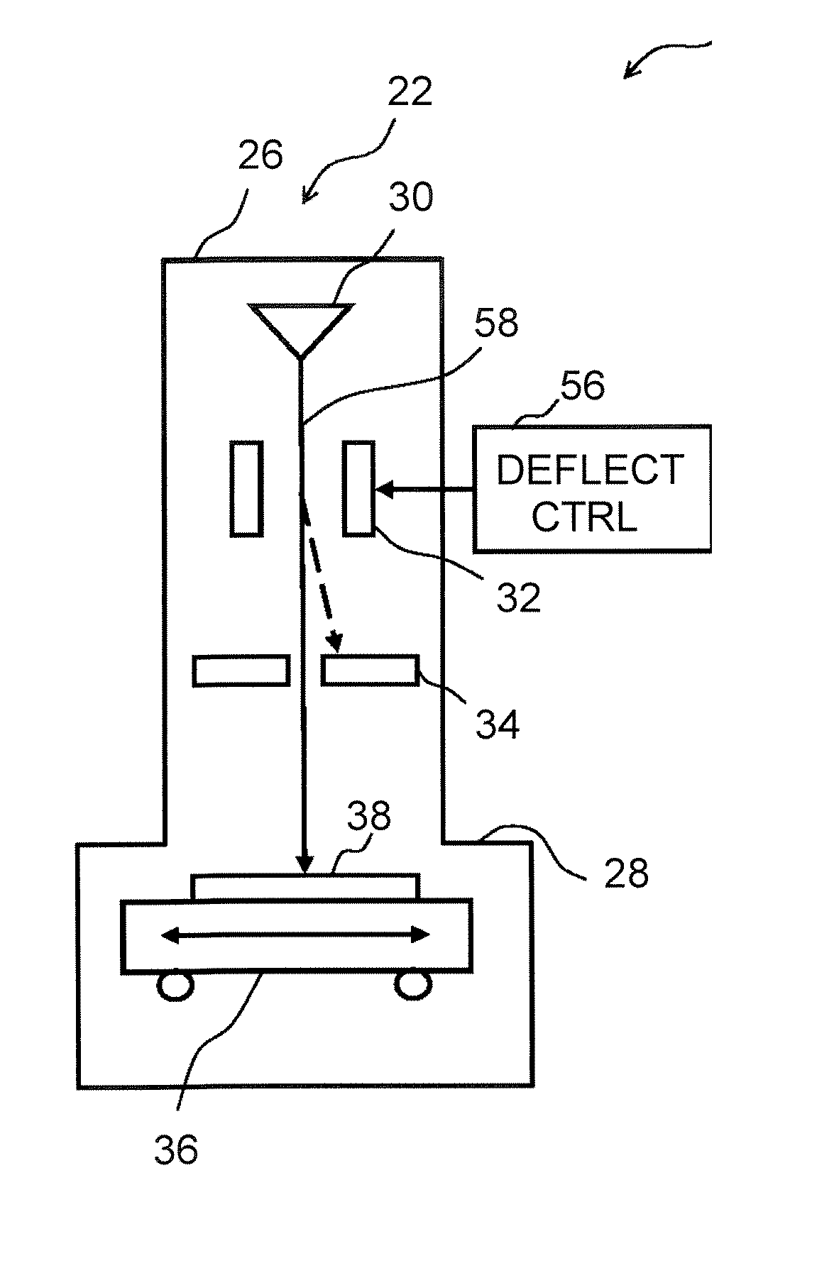
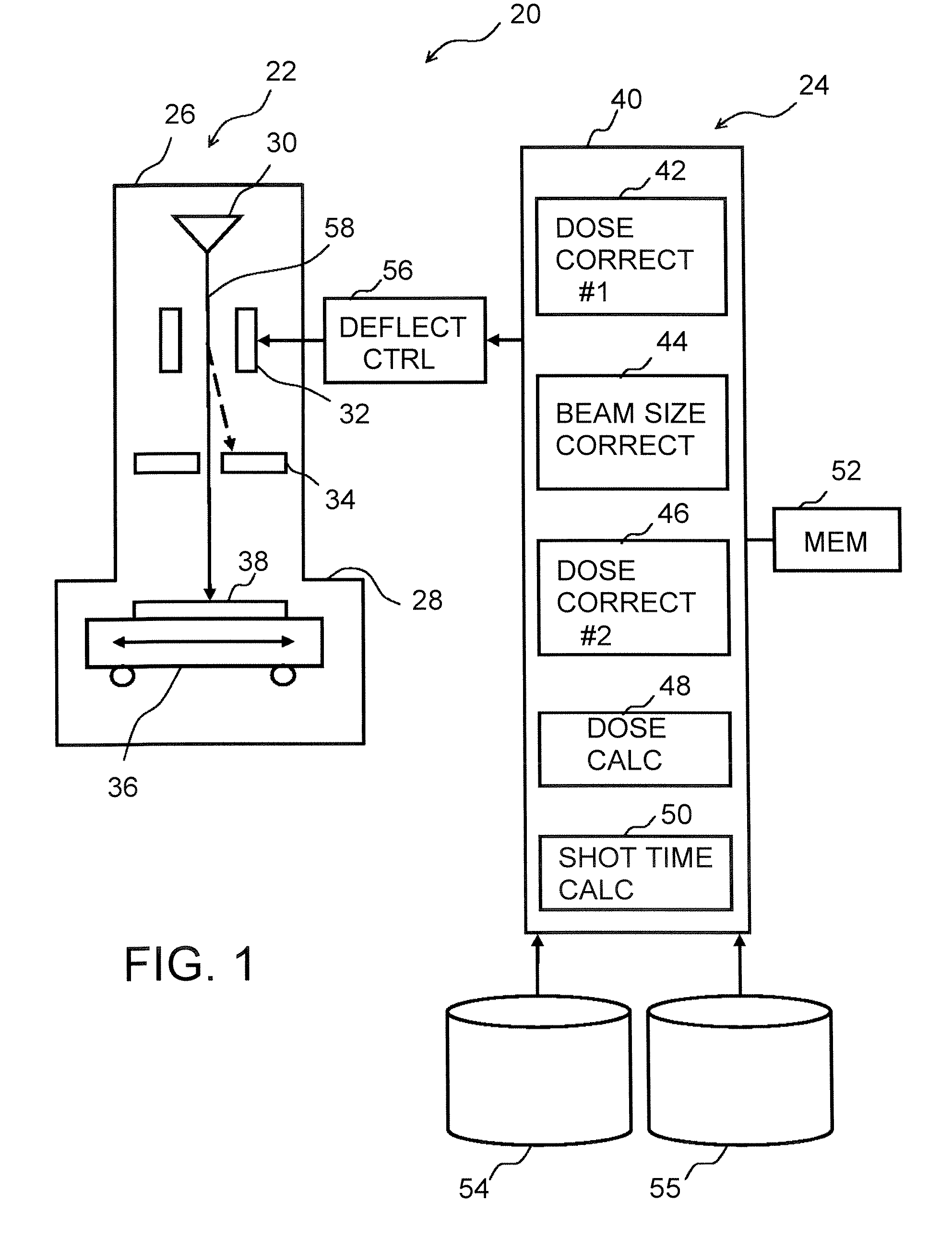
[0027] A variable-shaped electron beam (EB) pattern lithography apparatus embodying the invention is shown in FIG. 1, with some main components thereof being illustrated therein. As shown in FIG. 1, this EB lithography apparatus is wholly indicated by reference numeral 20. EB lithography apparatus 20 is generally made up of a circuit pattern drawing or “writing” unit 22 and a control unit 24 which is operatively associated therewith.

[0028] The pattern write unit 22 includes a tower-like outer housing structure 26, called an electron lens barrel, and a processing chamber 28. Electron lens barrel 26 has a scanning electron beam pattern generation unit as built therein. This unit is constituted from a variable-shaped electron beam column, which includes an electron gun assembly 30, a blanking deflector 32, and a blanking aperture plate 34. In the process chamber 28, a table-like structure 36 is situated which is movable in two orthogonal axes that define a horizontal plane, i.e., X ax...


PUM


Abstract

A beam dose computing method includes specifying a matrix of rows and columns of regions as divided from a surface area of a target object to include first, second and third regions of different sizes, the third regions being less in size than the first and second regions, determining first corrected doses of a charged particle beam for correcting fogging effects in the first regions, determining corrected size values for correcting pattern line width deviations occurring due to loading effects in the second regions, using said corrected size values in said second regions to create a map of base doses of the beam in respective ones of said second regions, using said corrected size values to prepare a map of proximity effect correction coefficients in respective ones of said second regions, using the maps to determine second corrected doses of said beam for correction of proximity effects in said third regions, and using the first and second corrected doses to determine an actual beam dose at each position on the surface of said object.

Description

CROSS-REFERENCE TO RELATED APPLICATION(S) [0001] This application claims priority to Japanese Patent Application No. 2005-309247, filed Oct. 25, 2005, the disclosure of which is incorporated herein by reference. FIELD OF THE INVENTION [0002] The present invention relates generally to energy radiation lithography technologies and, more particularly, to a technique for determining through computation the optimal dose of a charged particle beam as used to draw or “write” a pattern on a target object to thereby increase the line-width uniformity or homogeneity of the pattern. This invention also relates to microlithographic apparatus and methodology using the beam dose computation technique. DESCRIPTION OF RELATED ART [0003] With further advances in miniaturization of highly integrated semiconductor devices, microlithography techniques for generation and depiction of extra-fine patterns are becoming important more and more. In recent years, semiconductor circuit devices decrease in mini...

Claims


Application Information

Patent Timeline
Patent Type & Authority Applications(United States)
IPC IPC(8): A61N5/00H01J37/305H01L21/027
CPCB82Y10/00B82Y40/00G03F7/2061H01J37/3174H01J2237/31764H01J2237/31769G03F7/2059G03F7/70441
Inventor EMI, KEIKOSUZUKI, JUNICHIABE, TAKAYUKIIIJIMA, TOMOHIROYASHIMA, JUN
Owner NUFLARE TECH INC
Why Eureka
Try Eureka