Field effect transistor and method of manufacturing the same

a field effect transistor and field effect technology, applied in the field of thin film transistors, can solve the problems of inability to improve the device characteristic of the tft, the uniformity of the characteristics of the respective device, and the inability to control the size or orientation of the formed semiconductor grains, etc., to achieve the effect of improving the mobility of carriers, facilitating the formation of plural organic tfts, and reducing the cost o

Inactive Publication Date: 2007-05-24
HITACHI LTD
View PDF4 Cites 51 Cited by
  • Summary
  • Abstract
  • Description
  • Claims
  • Application Information

AI Technical Summary

Benefits of technology

[0015] According to an aspect of the present invention, semiconductor organic molecule solution on the substrate is dried anisotropcally by using a pattern of a type which is given to the substrate, thereby making it possible to control the growth direction or orientation of the grains that form the organic molecular crystal thin film which grows from the solution. As a result, it is possible to improve the mobility of carriers that flow in the channel. In the case where the semiconductor organic molecular crystal is made to grow from the liquid, in order to realize the control of the orientation of crystal or the growth direction inexpensively, it is necessary to control the drying process of the solution in which the semiconductor organic molecules are solved. In order to achieve this object inexpensively, it is most realistic to use a pattern that is given to the substrate. Through the above method, it is possible to inexpensively and readily form plural organic TFTs that are large in the carrier mobility on the same substrate through a printing process including a coating method or an ink jet method.

Problems solved by technology

However, all of the above problems cannot be solved by the above coating technique.
Also, it has not been possible to control the size or orientation of the grains of the formed semiconductor.
Therefore, it is difficult to improve the device characteristic of the TFT and the uniformity of the characteristics in the respective devices as well as the reliability.

Method used


Image

  • Field effect transistor and method of manufacturing the same
  • Field effect transistor and method of manufacturing the same
  • Field effect transistor and method of manufacturing the same

Examples


first embodiment

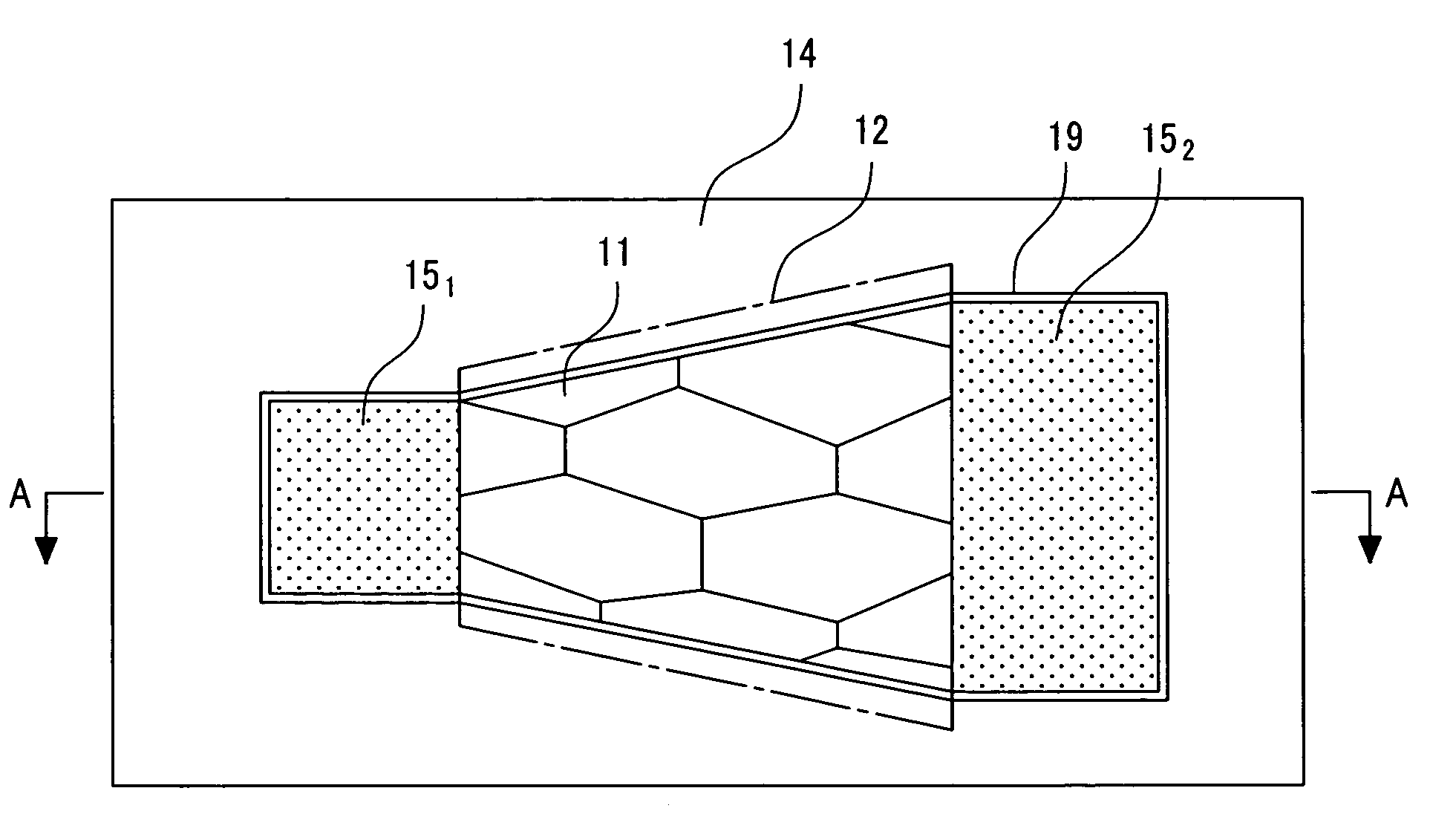
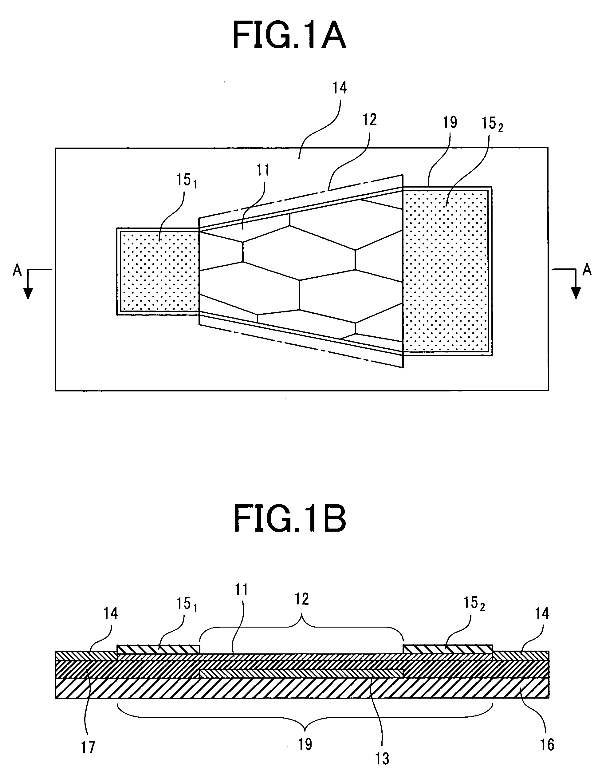
[0029]FIG. 1A is a plan schematically showing the structure of a TFT according to a first embodiment of the present invention. FIG. 1B is a cross-sectional view taken along an arrow direction at a position A-A of FIG. 1A.

[0030] Referring to FIG. 1A, reference numeral 151 and 152 denote source and drain electrodes, respectively. Reference numeral 11 is a semiconductor organic molecular crystal thin film that consists of highly oriented grains and constitutes a channel region 12 of the TFT. Reference numeral 14 is a region that is high in the solution lyophobic property, and reference numeral 19 is a lyophilic region (a region that is low in the lyophilicity). The present invention defines a drying direction of the semiconductor organic molecule solution that is supplied to the lyophilic region 19, and controls the orientation and grain size of the growing crystal by using a pattern of the lyophilic region 19 within a region surrounded by the lyophobic region 14 as will be described ...

second embodiment

[0040]FIG. 4 is a plan schematically showing a second embodiment in which plural channels 12 are formed on the substrate by combination of plural regions that are arranged in parallel with the drain electrodes 151 and 152. An example of FIG. 4 is identical with the first embodiment in that the lyophilic region 19 is disposed in the lyophobic region 14, and the channel 12 and the source and drain electrodes 151 and 152 at both sides of the channel 12 are formed in the lyophilic region 19. However, the example of FIG. 4 is different from the first embodiment in that the plural channels 12 that change their widths along the longitudinal axial direction as in the first embodiment are formed in parallel with the channel region 12′. The channel region 12′ is not entirely formed by the lyophilic region, but formed by having plural rectangular lyophobic regions 14 remaining which are narrower in the width and mutually inclining by a given angle. Therefore, the plural lyophilic regions that ...

third embodiment

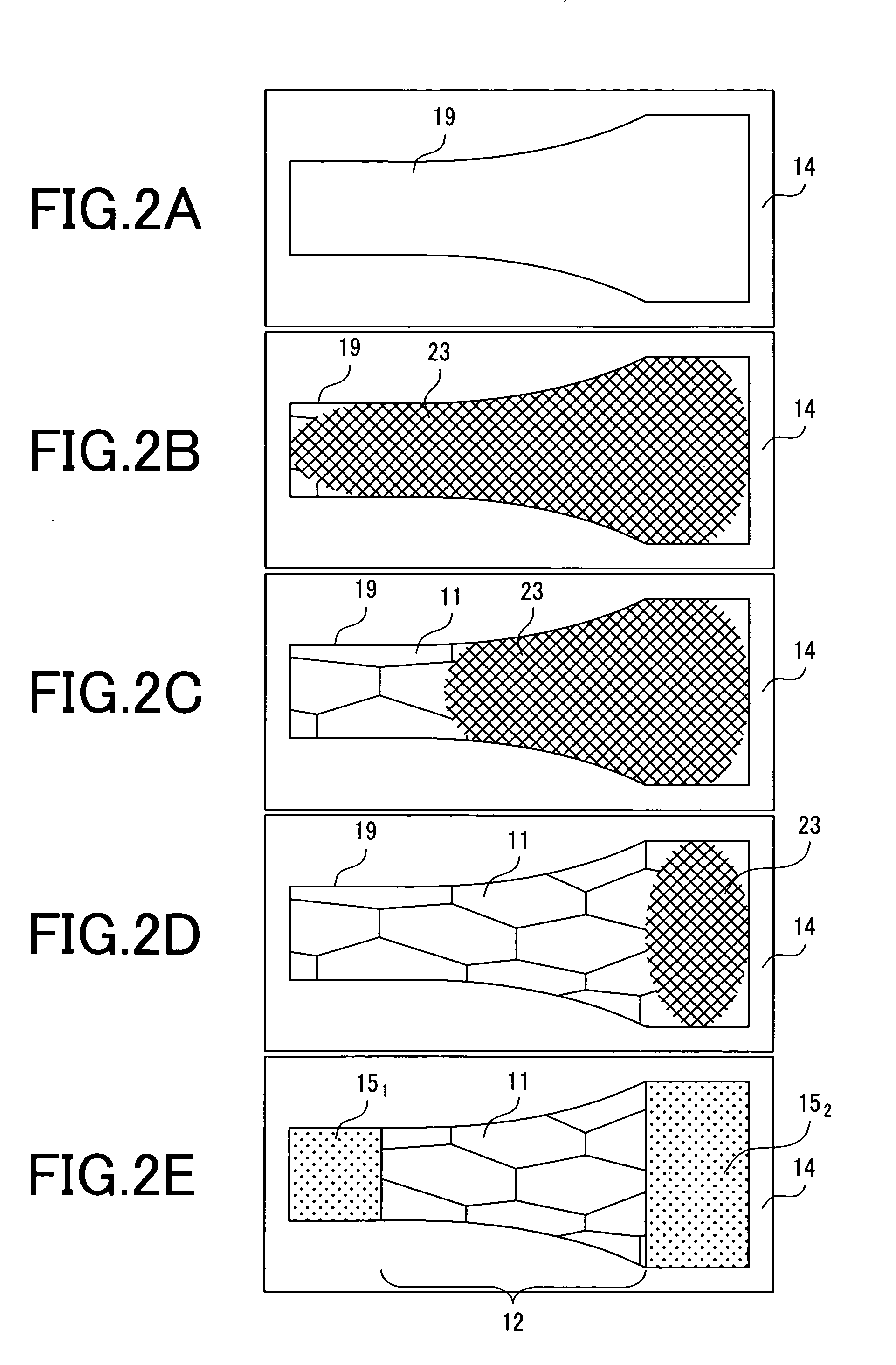
[0043]FIGS. 5A to 5E are diagrams showing specific examples in which the TFT according to the present invention is made of an inorganic material except for the semiconductor organic molecular crystal thin film of the channel, and has a structure having the channels 12 shown in FIG. 4. In each of FIGS. 5A to 5E, the left side shows a cross-sectional view, and the right side shows a plan.

[0044] As shown in FIG. 5A, a gate electrode 13 is formed on a silicon substrate 16. For that reason, a thermally oxidized film 17 is formed on the silicon substrate 16, and an aluminum thin film that is 30 nm in the thickness is formed on the thermally oxidized film 17 by sputtering vapor deposition to provide the gate electrode 13. The size of the gate electrode 13 corresponds to 500 μm in the channel length and 500 μm in the channel width.

[0045] Then, as shown in FIG. 5B, an oxide silicon insulating film 51 that is 20 nm in the thickness is formed on the gate electrode 13 by sputtering vapor depo...


PUM


Abstract

A TFT having a large mobility of carriers that are conducted through a channel as compared with a conventional organic TFT, and a method of manufacturing the TFT inexpensively and easily are provided. The channel is formed of a semiconductor organic molecular crystal thin film which is highly oriented, and a TFT that is large in the mobility of the carriers that are conducted through the channel, and a lyophilic TFT pattern that is surrounded by a lyophobic region on a substrate are formed, and the configuration of the pattern is featured, whereby a solution of the semiconductor organic molecules which is supplied to an appropriate region of a substrate surface including the channel is spontaneously dried in an anisotropic fashion, and highly oriented crystal is grown in the drying process.

Description

CLAIM OF PRIORITY [0001] The present application claims priority from Japanese Application JP2005-336709 filed on Nov. 22, 2005, the content of which is hereby incorporated by reference into this application. BACKGROUND OF THE INVENTION [0002] 1. Field of the Invention [0003] The present invention relates to a thin film transistor using an organic semiconductor and a method of manufacturing the thin film transistor, and more particularly to a transistor having a structure in which an organic semiconductor that forms a channel is made of a single crystal or a polycrystal of organic molecules, and having a structure in which the orientation of the single crystal is directed to a specific direction with respect to a direction that connects electrodes on both ends of the channel to each other, or having a structure in which grains that constitute the polycrystal are arranged in a specific direction with respect to a direction that connects the electrodes on both ends of the channel to e...

Claims


Application Information

Patent Timeline
Patent Type & Authority Applications(United States)
IPC IPC(8): H01L21/8234
CPCH01L51/0003H01L51/0012H01L51/052H01L51/0545H10K71/191H10K71/12H10K10/471H10K10/466
Inventor FUJIMORI, MASAAKIHASHIZUME, TOMIHIROANDO, MASAHIKO
Owner HITACHI LTD
Why Eureka
Try Eureka