

Method and apparatus for evaluating pattern shape of a semiconductor device
a semiconductor device and pattern technology, applied in the field of method and apparatus for evaluating the pattern shape of a semiconductor device, can solve problems such as failure of automatic measurement, and achieve the effects of reducing the semiconductor pattern formation cycle time, effective semiconductor manufacturing, and easy selection
- Summary
- Abstract
- Description
- Claims
- Application Information
AI Technical Summary
Benefits of technology
Problems solved by technology
Method used
Image

Examples
Embodiment Construction
[0078] Hereinafter, embodiments of the present invention will be described in detail with reference to the accompanying drawings. Note that components having the same function are denoted by the same reference symbols throughout the drawings for describing the embodiment, and the repetitive description thereof will be omitted.
[0079] Although a semiconductor wafer (or abbreviated as just “wafer”) in which a pattern is formed will be described as a test sample for shape evaluation object using the critical dimension SEM, the present invention is not restricted to this example.
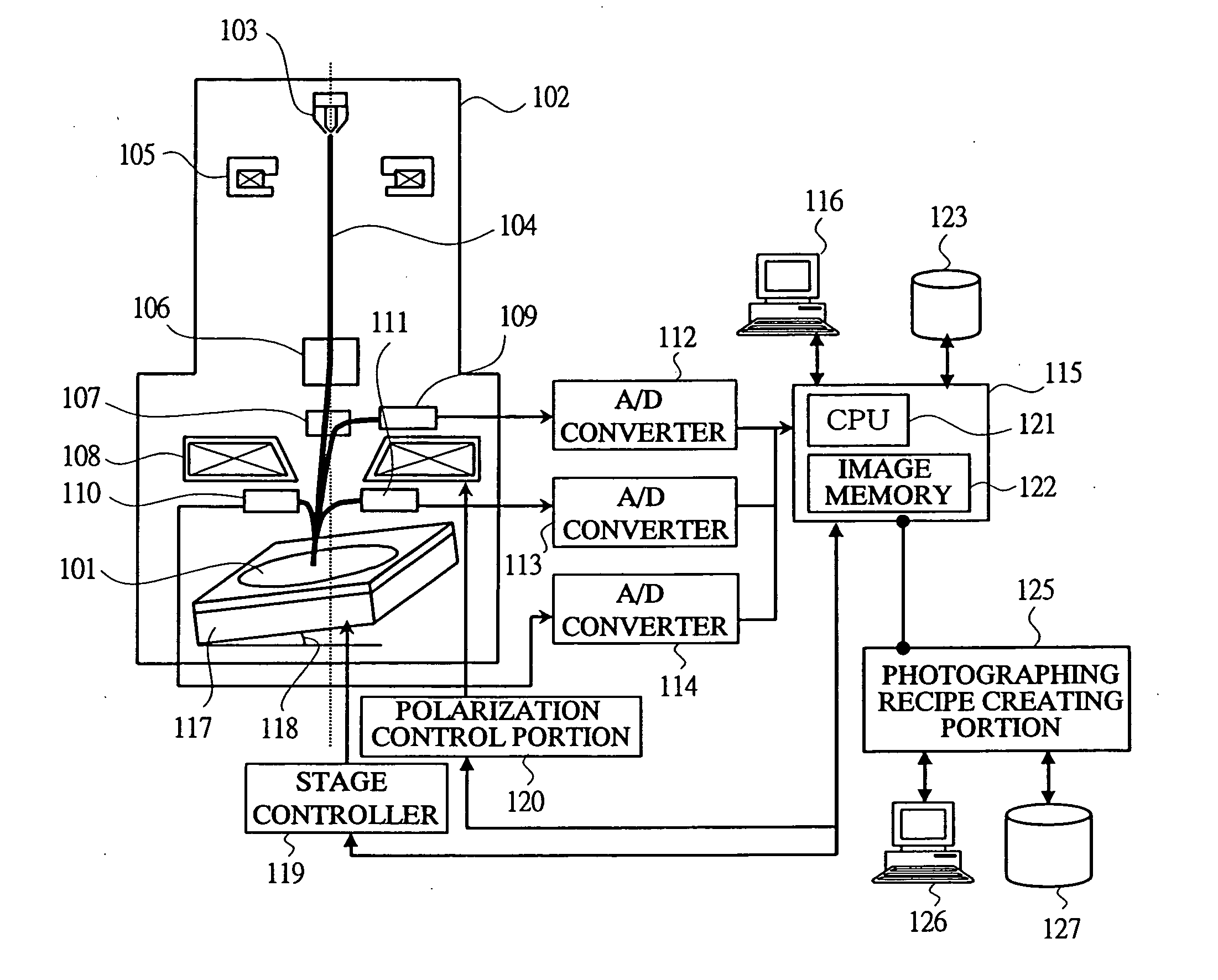
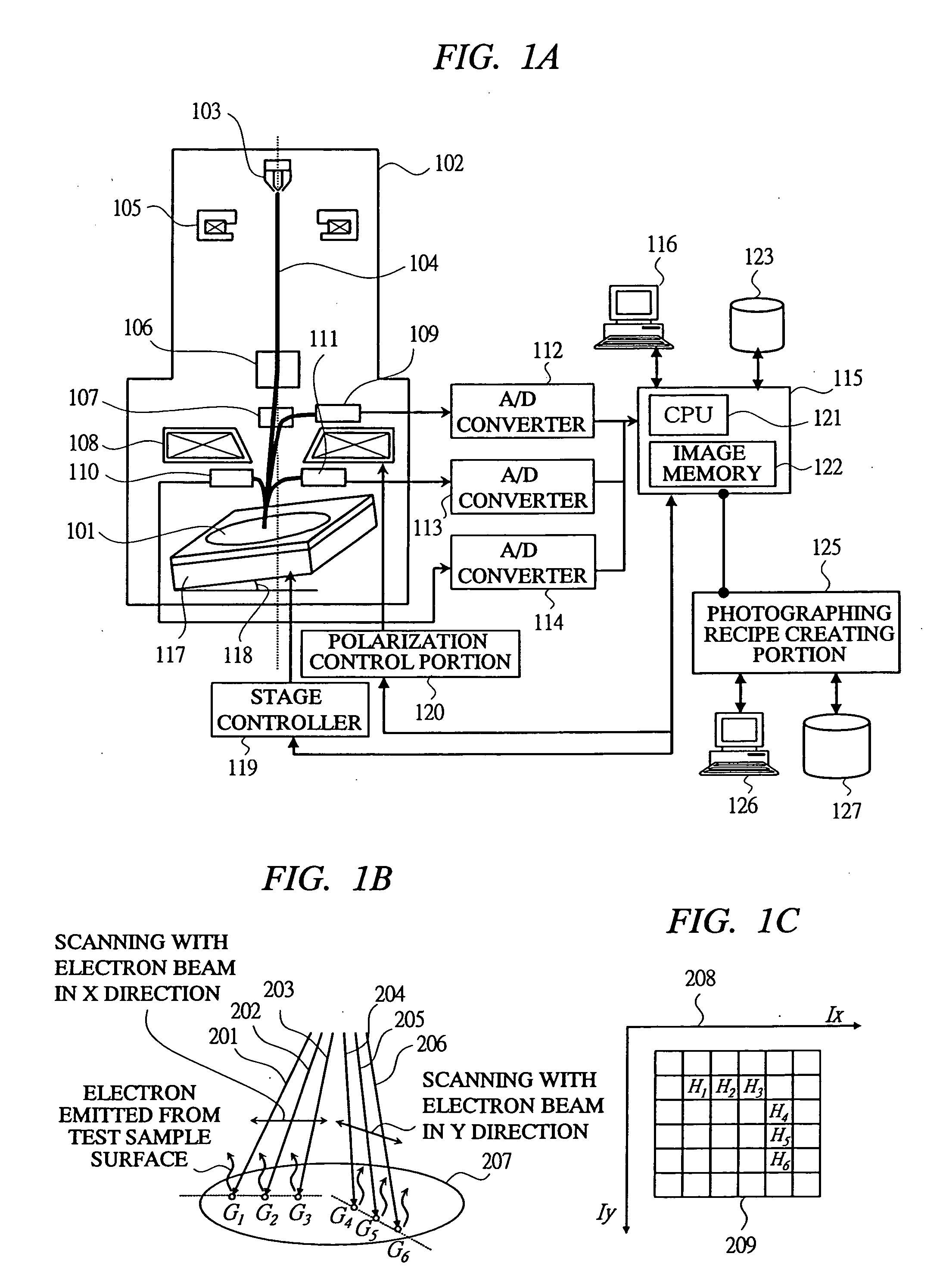
(Structure of Critical Dimension SEM: FIG. 1)
[0080]FIG. 1 is a drawing showing an example of system for achieving the semiconductor pattern shape evaluation method according to an embodiment of the present invention, FIG. 1A is a drawing showing particularly critical dimension SEM in detail, and FIGS. 1B, 1C are diagrams showing a method for converting the quantity of signals of electron emitted from the semi...
PUM
 Abstract
Description
Claims
Application Information