

Semiconductor device having super junction MOS transistor and method for manufacturing the same
- Summary
- Abstract
- Description
- Claims
- Application Information
AI Technical Summary
Benefits of technology
Problems solved by technology
Method used
Image

Examples
Embodiment Construction
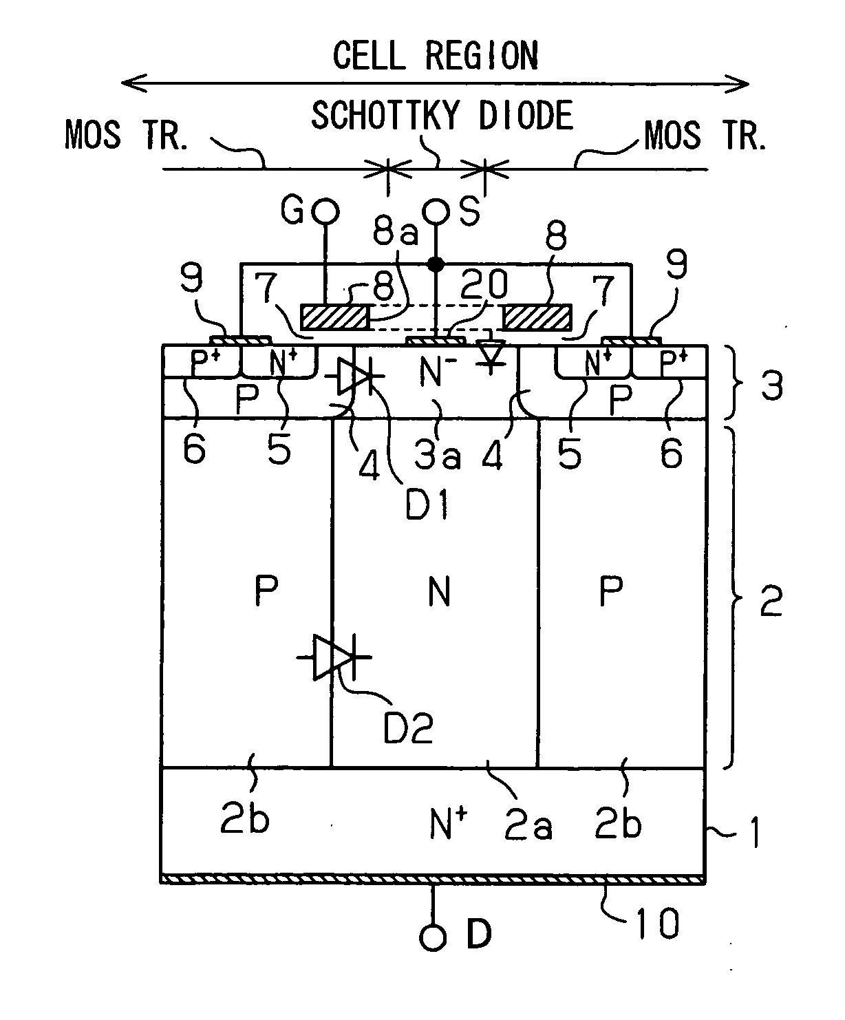
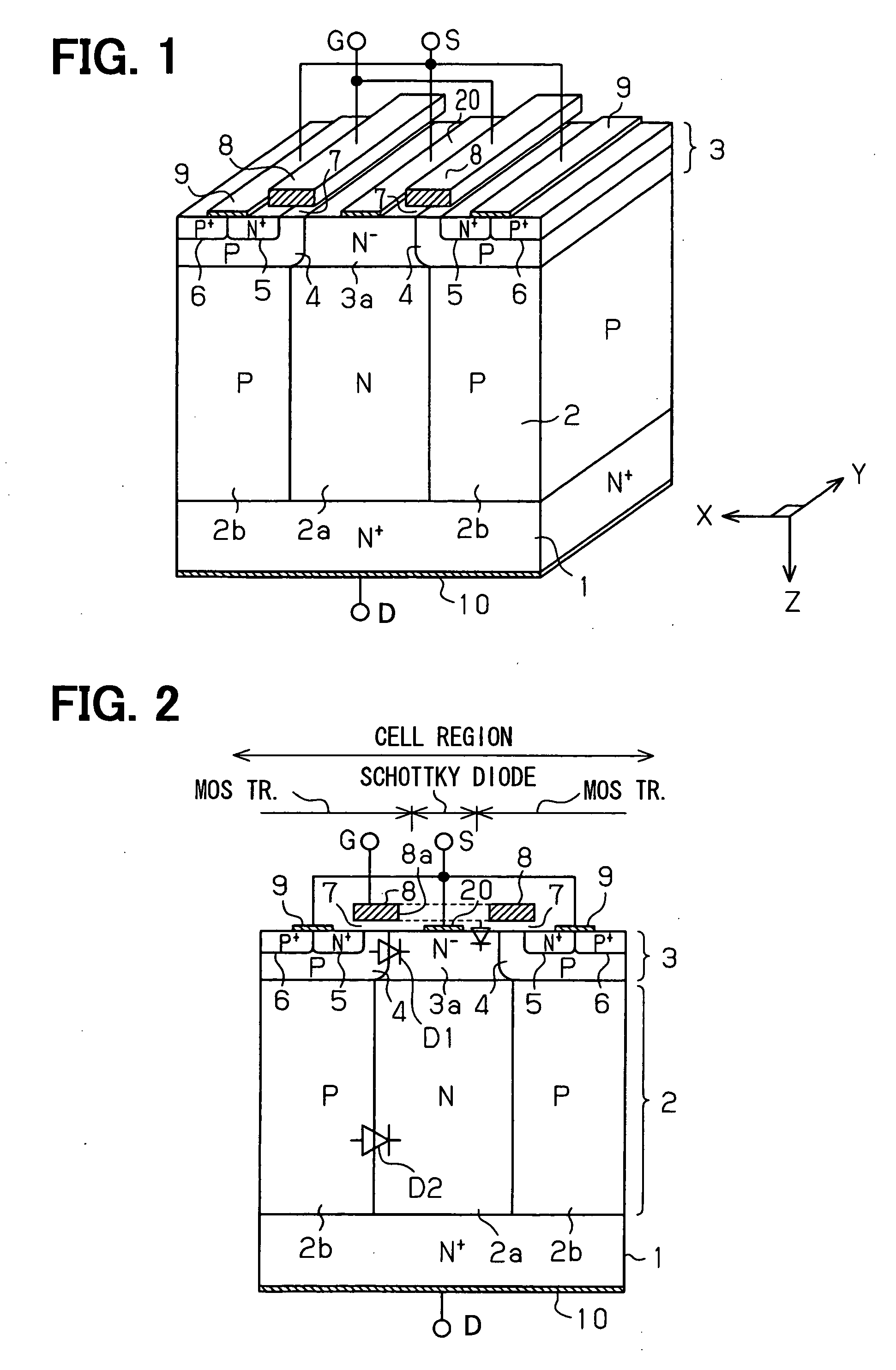
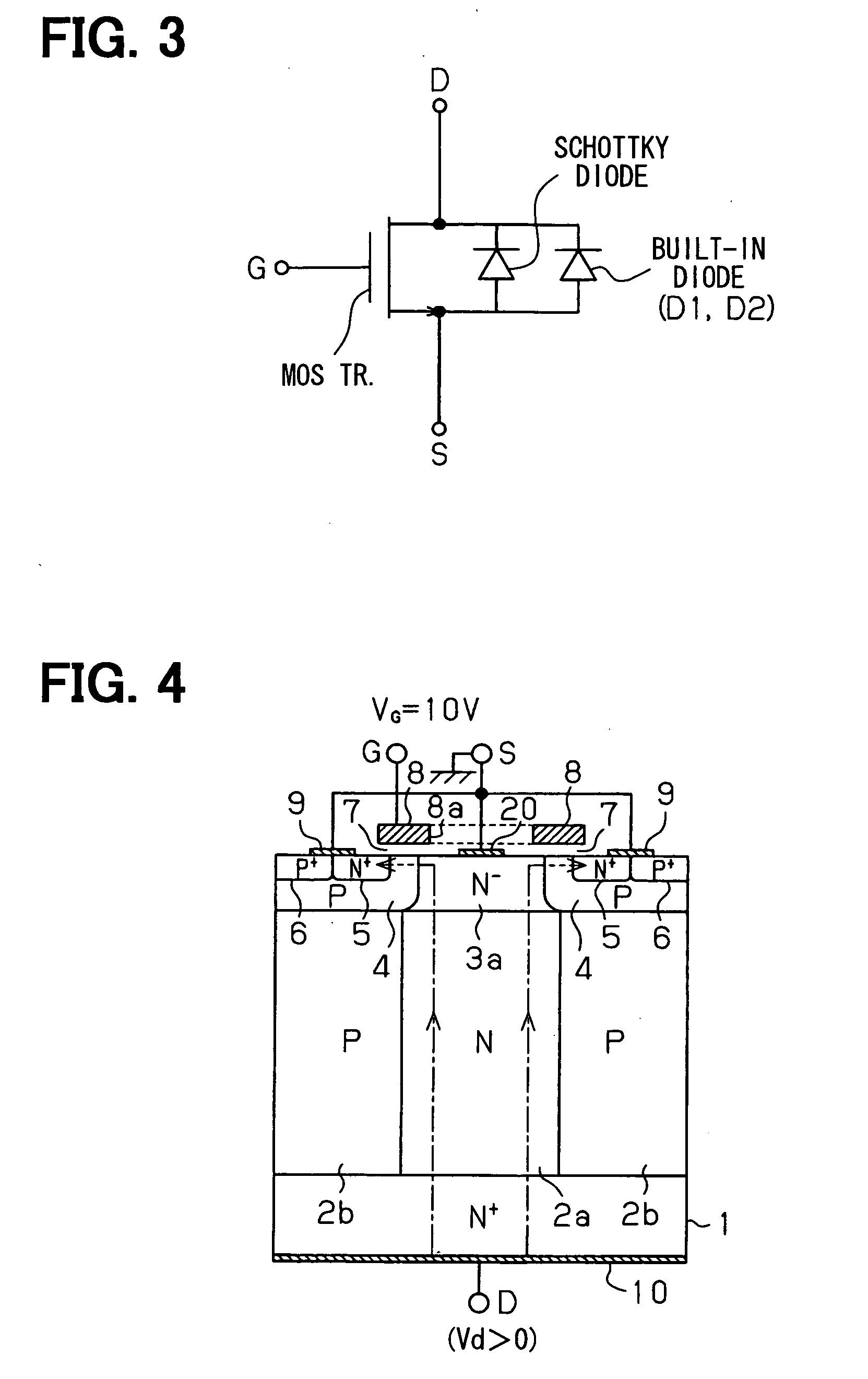
[0055]FIG. 1 shows a perspective view of a semiconductor device in this embodiment mode. FIG. 2 shows a longitudinal sectional view of the semiconductor device in this embodiment mode. FIG. 3 shows an equivalent circuit.
[0056] This semiconductor device is a semiconductor device having a super junction MOS structure, and a super junction MOS transistor and a Schottky barrier diode are integrated. The MOS transistor is an N channel transistor.
[0057] A silicon layer 2 as a semiconductor layer is laminated on an N+ silicon substrate 1 as a high concentration semiconductor substrate of a first electric conductivity type. An impurity diffusive area 2a of an N type (first electric conductivity type) and an impurity diffusive area 2b of a P type (second electric conductivity type) as a drift area are adjacently alternately arranged in the silicon layer 2. Thus, the super junction structure is constructed by adjacently alternately arranging the N type impurity diffusive area 2a and the P t...
PUM
 Abstract
Description
Claims
Application Information